《走进 TPU 与 GPU 集群:集合通信的解剖》中英对照全译
Aleksa Gordić 的长文《Inside TPU and GPU Clusters: The Anatomy of Collective Communication》全文对照翻译:左栏英文原文、右栏对应中文。从 TPU 的 2D/3D torus 与 GPU 的 fat tree 拓扑讲起,把 All-Gather、Reduce-Scatter、All-Reduce、All-to-All 的 ring/tree 实现、代价模型,以及 SHARP 与跨节点分层通信一次讲透。
原文:Inside TPU and GPU Clusters: The Anatomy of Collective Communication,作者 Aleksa Gordić。
本站是中英对照排版:左栏英文原文,右栏对应的中文译文。术语(All-Gather、Reduce-Scatter、All-Reduce、All-to-All、ICI、DCN、NVLink、SHARP、fat tree 等)保留英文写法;原文 35 张配图全部保留,并标注出处。
这篇长文从硬件拓扑讲起,把训练/推理里最核心的几个集合通信原语拆开讲透:TPU 的 2D/3D torus 与 GPU 的 fat tree,ring / tree 算法,All-Gather、Reduce-Scatter、All-Reduce、All-to-All 的具体实现与代价模型,以及 NVSwitch 上的 SHARP 和跨节点的分层集合通信。
In this post, I’ll do a deep dive into TPU and GPU cluster topologies, and cover the core collective operations used during transformer training and inference.
这篇文章会深入 TPU 和 GPU 的集群拓扑,并覆盖 transformer 训练与推理中最核心的那些集合通信操作。
Why should we care?
我们为什么要关心这个?
In 2026, training and serving transformers is a massively distributed systems problem.
在 2026 年,训练和推理 transformer 已经是一个彻头彻尾的分布式系统问题。
To shard models across a cluster, we rely on techniques such as data parallelism, tensor/model parallelism, FSDP, and expert parallelism. Under the hood, these techniques are built on a small set of core collective operations:
要把模型切分到一整个集群上,我们依赖数据并行、张量/模型并行、FSDP 和专家并行这类技术。而在底层,这些技术都构建在一小撮核心集合通信操作之上:
- Data parallel training requires gradient synchronization during backprop, this is typically implemented with all-reduce. As we’ll see later in this post, all-reduce itself can be decomposed into reduce-scatter followed by all-gather.
- Tensor parallelism and FSDP rely heavily on all-gather and reduce-scatter in the forward and backward passes.
- Expert parallelism, used in MoE models, rely on the all-to-all primitive.
- 数据并行训练需要在反向传播时同步梯度,通常用 all-reduce 实现。后面我们会看到,all-reduce 本身可以分解为 reduce-scatter 加 all-gather。
- 张量并行和 FSDP 在前向、反向传播中大量依赖 all-gather 和 reduce-scatter。
- MoE 模型用的专家并行,依赖 all-to-all 这个原语。
These are just a few important examples, but they’re enough to show why understanding collective communication is useful -> if you want to reason about the performance of modern transformer systems, you eventually have to reason about how data moves through the cluster.
这些只是几个重要例子,但已经足以说明为什么理解集合通信很有用 —— 如果你想推理现代 transformer 系统的性能,最终总得推理数据是怎么在集群里流动的。
We’ll start from the hardware, with the TPU and GPU cluster topologies. Understanding the physical layout of the cluster makes the collective algorithms much more grounded and easier to reason about.
我们会从硬件讲起,先看 TPU 和 GPU 的集群拓扑。理解了集群的物理布局,集合通信算法就会变得具体得多、也更好推理。
From there, we’ll dive into the most common implementations of the core collective operations.
之后,我们会深入这些核心集合通信操作最常见的实现方式。
I’ll focus primarily on ring-style algorithms, since they are the natural starting point for large-message communication.
我会主要讲 ring 风格的算法,因为它们是处理大消息时最自然的起点。
For smaller payloads, latency starts to dominate, and tree-style algorithms can be a better fit (as they require only log2 steps).
而对于较小的载荷,延迟开始占主导,tree 风格的算法可能更合适(它们只需要 log2 步)。
This post is structured into seven parts:
本文分成七个部分:
- TPU cluster topology: Superpods, Slices, DCN, PCIe, ICI
- Inside All-Gather: 1D/2D Rings, and Chains
- Reduce-Scatter (and All-Reduce): The Dual of All-Gather
- All-to-All: A Sharded Transpose
- NVIDIA GPU cluster topology: Nodes, Scalable Units, Fat Tree
- GPU Collectives Within the Node: Rings, Trees, and SHARP
- GPU Collectives Across Nodes: Hierarchical Algorithms over InfiniBand
- TPU cluster topology:Superpod、Slice、DCN、PCIe、ICI
- Inside All-Gather:1D/2D ring 与 chain
- Reduce-Scatter(以及 All-Reduce):All-Gather 的对偶
- All-to-All:一种分布式的转置
- NVIDIA GPU cluster topology:Node、Scalable Unit、Fat Tree
- GPU Collectives Within the Node:ring、tree 与 SHARP
- GPU Collectives Across Nodes:基于 InfiniBand 的分层算法
I’ll start with TPUs because their topology is more uniform, and therefore arguably easier to reason about, than GPU cluster topology.
我先从 TPU 讲起,因为它们的拓扑比 GPU 集群更规整,因此(可以说)更容易推理。
The key difference between TPU and GPU clusters is the nearest-neighbor connectivity. TPU chips are connected directly to neighboring TPU chips, and each chip has either 4 or 6 nearest neighbors, depending on the TPU generation:
TPU 和 GPU 集群的关键区别在于最近邻连接。TPU 芯片直接和相邻的 TPU 芯片相连,每颗芯片有 4 个或 6 个最近邻,取决于 TPU 的代次:
- TPU
v2,v3,v5e, andv6euse a 2D torus topology, with 4 nearest neighbors. - TPU
v4p,v5p,TPU7x(Ironwood), and8tuse a 3D torus topology, with 6 nearest neighbors.
- TPU
v2、v3、v5e和v6e使用 2D torus 拓扑,有 4 个最近邻。 - TPU
v4p、v5p、TPU7x(Ironwood)和8t使用 3D torus 拓扑,有 6 个最近邻。
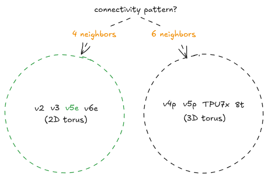
Figure 1: TPU connectivity classes
💡 Boardfly topology:
Notably, Google’s new inference TPU chip[1]
8ideviates from the 2D/3D torus, and instead uses boardfly, a hierarchical high-radix topology. In this post I’ll ignore it.
💡 Boardfly 拓扑:
值得注意的是,Google 新的推理 TPU 芯片[1]
8i偏离了 2D/3D torus,改用 boardfly——一种分层的 high-radix 拓扑。本文不涉及它。
Here is one way to build intuition for the 4-neighbor, 2D torus pattern. A 2D torus can be represented as a grid with wraparound/periodic boundaries: moving off the left edge brings you back on the right edge (and vice versa), and moving off the top edge brings you back on the bottom edge (and vice versa). Bear in mind that the TPU torus is a discrete grid; imagine it overlaid on this donut. The visualization is just for intuition:
下面是一种建立 4 邻居 2D torus 直觉的方式。2D torus 可以看成一个带环绕/周期边界的网格:从左边走出去会从右边回来(反之亦然),从上边走会从下边回来(反之亦然)。请记住,TPU 的 torus 是一个离散网格;把它想象成叠在这个甜甜圈上就好。这张图只是为了建立直觉:
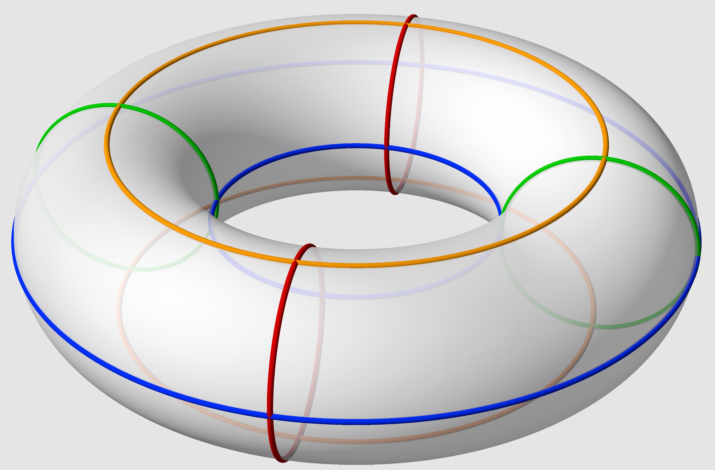
Figure 2: 2D torus intuition: a grid with wraparound boundaries
Similarly, here is the 6-neighbor, 3D torus connectivity pattern:
同样地,这是 6 邻居 3D torus 的连接模式:
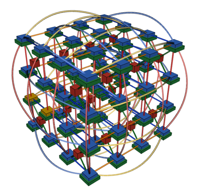
Figure 3: 3D torus connectivity
This looks a bit messy, but the idea is simple -> each chip has neighbors along ±x, ±y, and ±z, and the edges wrap around in all three dimensions.
看起来有点乱,但思路很简单 —— 每颗芯片沿着 ±x、±y、±z 都有邻居,三个维度上边界都环绕。
💡 Interactive Visualization Tool:
Here is a neat little visualization tool[2] I used to generate the above image, you can use it to interact with these more complex topologies.
We’ll use v5e as the running example in this post, since 2D connectivity is easier to visualize.
本文用 v5e 作为贯穿全文的例子,因为 2D 连接更好画。
TPU chips communicate with their neighbors over ICI, short for inter-chip interconnect.
TPU 芯片之间通过 ICI(inter-chip interconnect,片间互联)通信。
The largest ICI-connected island of TPU chips is called a TPU Pod. You’ll also sometimes hear people refer to this as a “superpod”; I’ll use the terms interchangeably here.
通过 ICI 连在一起的最大一片 TPU 芯片,叫做一个 TPU Pod。你有时也会听到人们把它叫做 “superpod”;本文中这两个词混用。
For example, a v4 pod contains 16 × 16 × 16 chips, for a total of 4096 TPUs. A v5p pod contains 16 × 20 × 28 chips, or 8960 TPUs!
例如,一个 v4 pod 包含 16 × 16 × 16 颗芯片,总共 4096 颗 TPU。一个 v5p pod 包含 16 × 20 × 28 颗芯片,也就是 8960 颗 TPU!
💡 GPUs scale-up domains:
Contrast this with GPUs, where the scale-up domain has traditionally been much smaller: commonly 8 GPUs in a single NVLink domain, and more recently 72 GPUs in an NVLink domain with NVIDIA GB200 NVL72. We’ll analyze GPUs in much more depth a bit later.
💡 GPU 的 scale-up 域:
对比之下,GPU 的 scale-up 域历来小得多:常见的是单个 NVLink 域里 8 张 GPU,最近 NVIDIA GB200 NVL72 做到了一个 NVLink 域 72 张 GPU。GPU 我们稍后会讲得更细。
For TPU pods whose chips have 6 neighbors,the smallest full 3D torus is a 4×4×4 cube. If you request a smaller topology, for example 2×2×2, you lose the wraparound links, so the slice stops being a torus and becomes a mesh.
对于邻居数为 6 的 TPU pod,最小的完整 3D torus 是 4×4×4 的立方体。如果你申请更小的拓扑,比如 2×2×2,环绕链路就没了,这个 slice 也就不再是 torus,而变成了 mesh。
💡 Terminology:
A TPU slice is a collection of chips within a single TPU Pod connected through ICIs (an “ICI-island”). For
v5ethose can be: 2×2, 2×4, 8×8, etc. The largest such slice is the (super)pod itself.
💡 术语:
一个 TPU slice 是单个 TPU Pod 内通过 ICI 相连的一批芯片(一个 “ICI-island”)。对
v5e来说,可以是 2×2、2×4、8×8 等等。最大的这类 slice 就是(super)pod 本身。
This can roughly double the time of ring-style collectives along that axis, as we’ll soon see. So this is something to be aware of - if your application is communication-heavy, you may want to request slice shapes that preserve the torus structure, for example 4×4×8.
这会沿着该轴把 ring 风格集合通信的时间大致翻倍,后面我们就会看到。所以这是需要注意的一点 —— 如果你的应用是通信密集型的,你可能希望申请的 slice 形状能保住 torus 结构,比如 4×4×8。
v5e, on the other hand, has a 16×16 2D torus pod. The wraparound exists at size 16, so if you take a smaller slice, such as 8×16, you lose the wraparound along the shorter axis (again, collective ops along that axis pay roughly a 2× penalty).
而 v5e 是 16×16 的 2D torus pod。环绕存在于尺寸 16 上,所以如果你取一个更小的 slice,比如 8×16,短的那个轴上就失去了环绕(同样,沿该轴的集合通信要付出大约 2× 的代价)。
To scale beyond a single pod, TPUs use DCN, short for data center networking. DCN has much lower throughput than ICI, so you have to be careful: if too much communication crosses pod boundaries, it can easily become the bottleneck during training.
要扩展到单个 pod 之外,TPU 用的是 DCN(data center networking,数据中心网络)。DCN 的吞吐远低于 ICI,所以必须小心:如果有太多通信跨 pod 边界,它很容易成为训练时的瓶颈。
Putting all of that together, let’s visualize the topology of a 16×16 v5e pod. Spend some time analyzing this (zoom in if needed):
把这些拼在一起,我们来可视化一个 16×16 的 v5e pod 的拓扑。请花点时间分析(需要的话放大看):
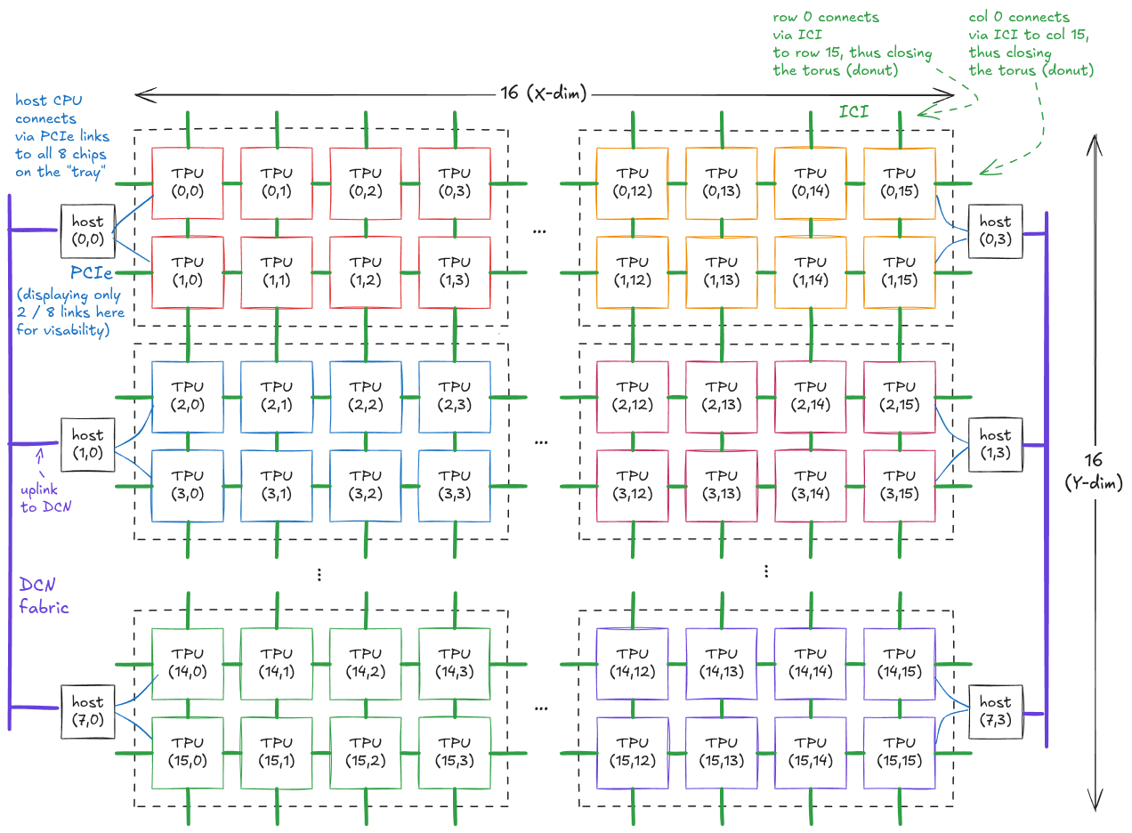
Figure 4: Topology of a v5e TPU 16x16 superpod
We can connect multiple pods into an even larger compute cluster through a shared DCN fabric (maybe this is what we should call a superpod, heh):
我们还可以通过一个共享的 DCN fabric 把多个 pod 连成更大的计算集群(也许这才该叫 superpod,哈):
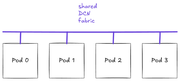
Figure 5: Multiple pods connected through a DCN backbone
A few more details are worth knowing.
还有几个细节值得知道。
As can be seen in the figure above, within the pod the 0th row connects back to the 15th row, and the 0th column connects back to the 15th column. This is what makes the topology a torus/donut instead of a regular mesh. The torus geometry constrains path lengths, because data often has to flow through intermediate TPUs to get from the source chip to the target chip.
如上图所示,在 pod 内部,第 0 行会连回第 15 行,第 0 列会连回第 15 列。这正是让拓扑成为 torus/甜甜圈而不是普通 mesh 的原因。torus 的几何形状约束了路径长度,因为数据常常要穿过中间的 TPU 才能从源芯片到达目标芯片。
For example, if TPU (15, 15) wants to send data to TPU (2, 15), the shortest path goes through the wraparound link:
比如,如果 TPU (15, 15) 想把数据发给 TPU (2, 15),最短路径会走环绕链路:
(15, 15) → (0, 15) →(1, 15) → (2, 15)
instead of going the long way through (14, 15), (13, 15), and so on.
而不是绕远路走 (14, 15)、(13, 15) 等等。
💡 Extra info:
TPUs also support “twisted torus” configurations, which alter the wraparound connectivity to reduce hop counts for communication patterns such as All-to-All. This is an implementation detail that improves efficiency, but we don’t need it for the purposes of this post.
💡 补充信息:
TPU 还支持 “twisted torus” 配置,它会改变环绕连接方式,以减少 All-to-All 这类通信模式的跳数。这是一个提升效率的实现细节,但本文用不到。
Each TPU chip is also connected to a “dedicated” CPU host through PCIe. In the case of v5e, one host is connected to a 2×4 block of TPU chips, giving us 8 PCIe connections between the host and those 8 chips.
每颗 TPU 芯片还通过 PCIe 连接到一台“专属”的 CPU 主机。以 v5e 为例,一台主机连接到一个 2×4 的 TPU 芯片块,也就是主机和这 8 颗芯片之间有 8 条 PCIe 连接。
Importantly, notice that to reach the DCN backbone, data has to flow through PCIe first, which means DCN communication is even slower than PCIe.
重要的是:注意要到达 DCN 骨干,数据必须先经过 PCIe,这意味着 DCN 通信甚至比 PCIe 还慢。
Concretely, cross-pod data flows from the source TPU chip’s HBM, over PCIe to the source host, then egresses over the DCN fabric, ingresses into the target host, and finally goes back over PCIe into the target TPU chip’s HBM.
具体来说,跨 pod 的数据流是:从源 TPU 芯片的 HBM,经 PCIe 到源主机,然后从 DCN fabric 出去,进入目标主机,最后再经 PCIe 回到目标 TPU 芯片的 HBM。
This gives us a natural bandwidth hierarchy. The closer we are to the compute die on the TPU chip, the faster the data movement is; the farther we move out into the cluster, the slower it gets.
这给了我们一个天然的带宽层级。离 TPU 芯片上的计算 die 越近,数据搬运越快;越往外走到集群里,就越慢。
Let’s put the relevant v5e cluster bandwidths on one picture:
我们把 v5e 集群里相关的带宽放到一张图上:
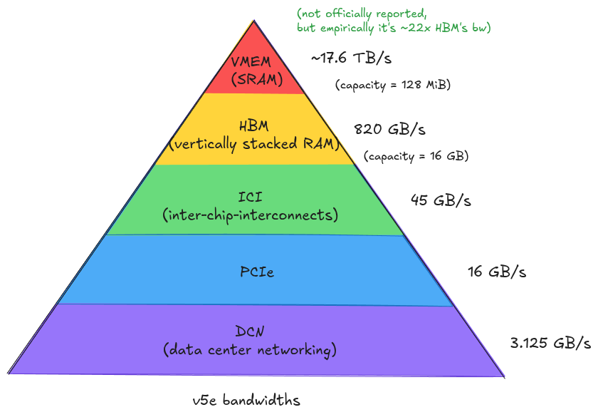
Figure 6: Bandwidth hierarchy in a v5e TPU cluster
Now that we have the topology and bandwidth hierarchy in mind, let’s look at a few concrete examples of how data actually flows through a TPU slice.
现在拓扑和带宽层级都在脑子里了,我们来看几个数据实际如何在 TPU slice 里流动的具体例子。
💡 Book recommendation:
A few of the examples in this blog, as well as the broader motivation for this post, were inspired by the excellent Scaling Book [3], which I highly recommend.
💡 书籍推荐:
本文中的一些例子,以及这篇文章更宏观的动机,都来自那本优秀的 Scaling Book [3],强烈推荐。
Suppose we request a 4×4 v5e slice from GCP. Since both axes are smaller than 16, we don’t get any wraparound links. So this slice is not a torus, it is a regular 2D grid, and some paths between chips are longer than they would be with wraparound links.
假设我们从 GCP 申请一个 4×4 的 v5e slice。由于两个轴都小于 16,我们拿不到任何环绕链路。所以这个 slice 不是 torus,而是普通的 2D 网格,芯片之间有些路径会比有环绕链路时更长。
Let’s pose the following question: how long does it take to move a (2048, 2048)``bf16 matrix from TPU chip (3, 3) to TPU chip (0, 0)?
那么提出这样一个问题:把一个 (2048, 2048) 的 bf16 矩阵从 TPU 芯片 (3, 3) 搬到 TPU 芯片 (0, 0) 需要多久?
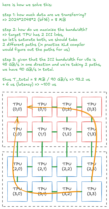
Figure 7: Moving an 8 MiB bf16 matrix across a 4×4 v5e mesh using two ICI paths
Note that we ignored link latency in the calculation above. In practice, ICI links have roughly 1 μs of latency per hop.
注意上面的计算里我们忽略了链路延迟。实践中,ICI 链路每一跳大约有 1 μs 的延迟。
In our example, each path is 6 hops long. Since the two paths run in parallel, this adds roughly 6 μs of latency to the transfer, which is negligible here, but may not be negligible for smaller messages.
在我们的例子里,每条路径长 6 跳。由于两条路径并行,这会给传输大约加上 6 μs 的延迟——在这里可以忽略,但对更小的消息就未必了。
This is why it’s important to understand whether we are in a latency-bound or throughput-bound regime.
这就是为什么必须搞清楚自己处在 latency-bound 还是 throughput-bound 的 regime。
A simple way to estimate this is to ask: assuming we saturate the unidirectional ICI bandwidth of 45 GB/s, how much data can flow through one link in 1 μs?
一个简单的估算方法是问:假设我们把单向 ICI 带宽 45 GB/s 打满,那么 1 μs 内一条链路上能流过多少数据?
The answer is:
答案是:
45 GB/s × 1 μs = 45 KB
So if our message chunks are around this size, latency matters a lot. Ignoring a 1 μs per-hop latency could make the estimate off by a large factor, so the simple bandwidth-only approximation is no longer valid.
所以如果你的消息分块大约是这个量级,延迟就非常关键。忽略每跳 1 μs 的延迟可能让估算差出一个很大的倍数,此时“只看带宽”的简单近似就不成立了。
Let’s do one more example, this time using PCIe, ICI, and HBM → VMEM links as well.
再做一个例子,这次把 PCIe、ICI 和 HBM → VMEM 这些链路都用上。
💡 what is VMEM?
VMEM is fast on-chip SRAM, roughly equivalent to programmer-managed shared memory on GPUs. It feeds directly into the matmul units; the systolic array, in the case of a TPU chip.
The details of the TPU chip are not important for understanding the main topic of this post, so we won’t spend more time on VMEM here.
💡 什么是 VMEM?
VMEM 是芯片上的高速 SRAM,大致相当于 GPU 上由程序员管理的 shared memory。它直接喂给矩阵乘单元——在 TPU 芯片里就是 systolic array。
TPU 芯片的细节对理解本文主题并不重要,所以这里不再在 VMEM 上花时间。
Assume we have a (128 * 1024, 128 * 1024) bf16 matrix sharded over a 4 × 4 TPU slice. Each chip therefore owns a (32 * 1024, 32 * 1024) submatrix (128/4=32).
假设我们有一个 (128 * 1024, 128 * 1024) 的 bf16 矩阵,切分在一块 4 × 4 的 TPU slice 上。于是每颗芯片拥有一个 (32 * 1024, 32 * 1024) 的子矩阵(128/4=32)。
Also assume these submatrices have been offloaded to host DRAM.
再假设这些子矩阵已经被卸载到主机 DRAM 上。
How long does it take to move all of this data to TPU (0, 0) and do a matmul with a (128 * 1024, 128) bf16 matrix?
把所有数据搬到 TPU (0, 0) 上、并与一个 (128 * 1024, 128) 的 bf16 矩阵做矩阵乘,需要多久?
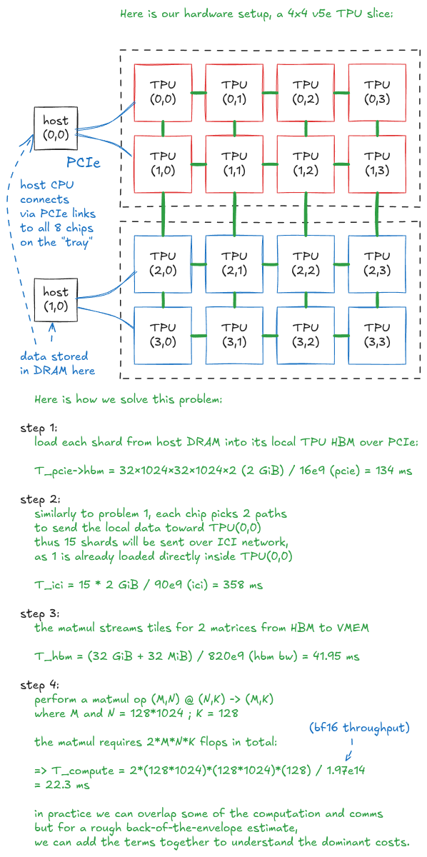
Figure 8: Gathering a sharded matrix onto TPU(0,0) for matmul
With the TPU topology and bandwidth hierarchy in mind, we’re ready to jump into collective operations.
TPU 的拓扑和带宽层级都清楚了,我们可以跳进集合通信操作了。
Let’s start with All-Gather.
先从 All-Gather 开始。
Let’s start with a motivating example.
先看一个动机例子。
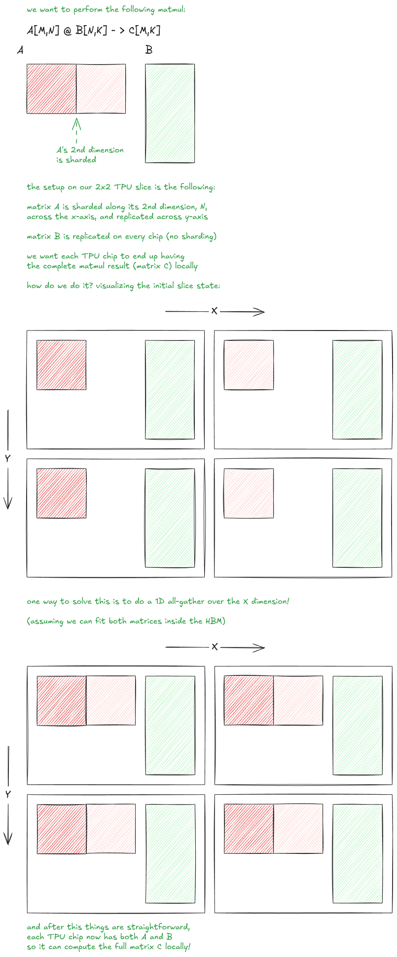
Figure 9: All-Gather motivation: gathering shards of A so each chip can run the matmul locally
So how do we efficiently implement All-Gather?
那我们怎么高效实现 All-Gather?
A common approach is to use a ring algorithm. Before looking at the algorithm itself, let’s first understand where this “ring” comes from:
常见做法是用 ring 算法。在看算法本身之前,先理解这个“ring”是从哪来的:
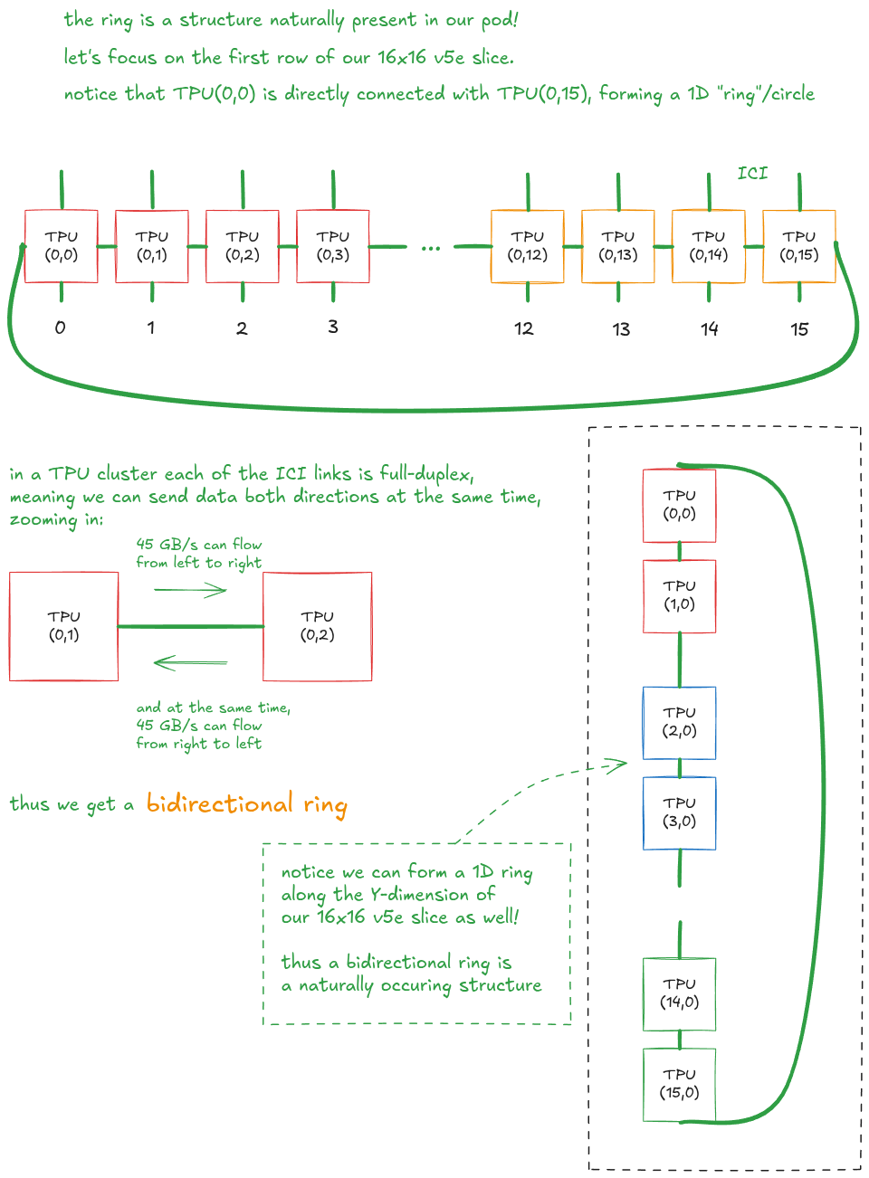
Figure 10: 1D bidirectional rings naturally appear along both axes of a 16×16 v5e torus
For easier visualization, let’s use a smaller ring of 8 TPU chips. In real v5e pods, the wraparound happens at size 16, but for the next few diagrams we’ll pretend that an 8-chip row also wraps around:
为了画起来简单,我们先用一个 8 颗 TPU 芯片的小 ring。真实的 v5e pod 里环绕发生在尺寸 16 上,但下面几张图我们先假装 8 颗芯片一行也会环绕:
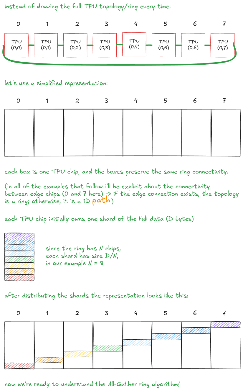
Figure 11: Simplified representation of an 8-chip ring
Here is All-Gather over a bidirectional 1D ring. It’s worth spending a bit of time on this diagram, zoom in and follow one shard as it moves around the ring:
这是双向 1D ring 上的 All-Gather。这张图值得花点时间,放大、跟着某一个分片沿着 ring 走一圈:
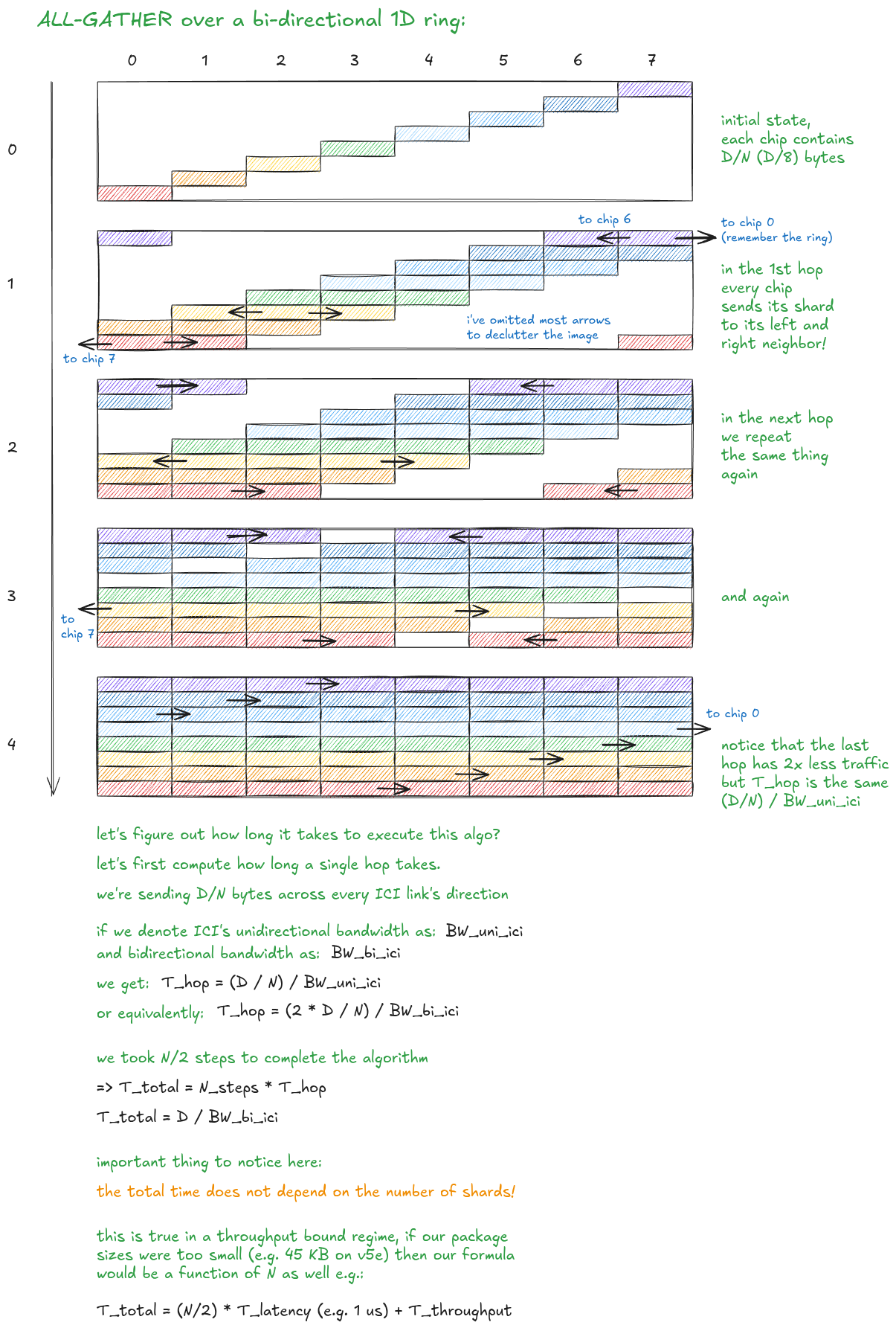
Figure 12: All-Gather over a bidirectional 1D ring
As an exercise, what would the algorithm look like if the ICI links were not full-duplex?
留个练习:如果 ICI 链路不是全双工的,算法会变成什么样?
In that case, we could run All-Gather over a unidirectional ring. To keep the diagram small, let’s use a hypothetical ring of size N = 4, so the algorithm completes in only N - 1 = 3 steps:
那种情况下,我们可以在单向 ring 上做 All-Gather。为了让图小一点,假设一个 N = 4 的 ring,于是算法只需要 N - 1 = 3 步就跑完:
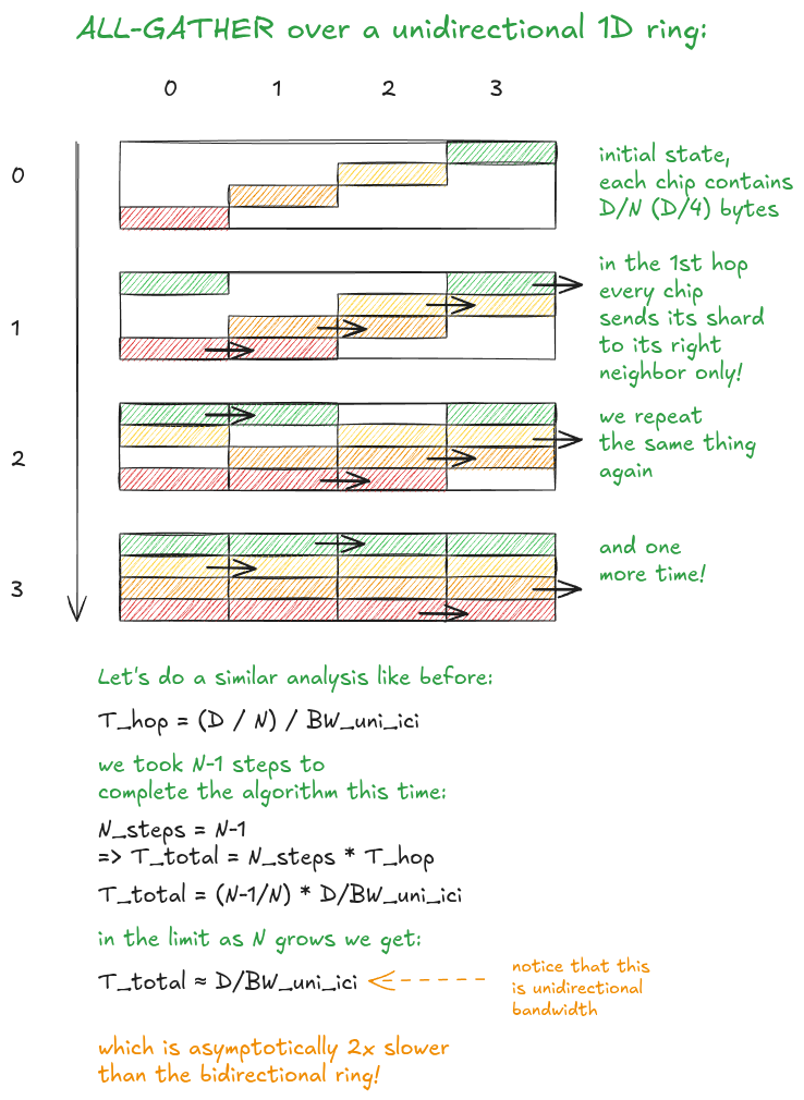
Figure 13: All-Gather over a unidirectional 1D ring
More realistically, if we take a TPU slice without wraparound links - for example, a 4 × 4 v5e slice - then we no longer have a ring along that axis. Instead, the topology becomes a 1D path, so we fall back to All-Gather over a path (or chain):
更贴近现实的情况是:如果我们取一个没有环绕链路的 TPU slice——比如 4 × 4 的 v5e slice——那么这个轴上就不再是 ring,而是一条 1D 路径,于是 All-Gather 退化成沿 path(或者说 chain)的 All-Gather:
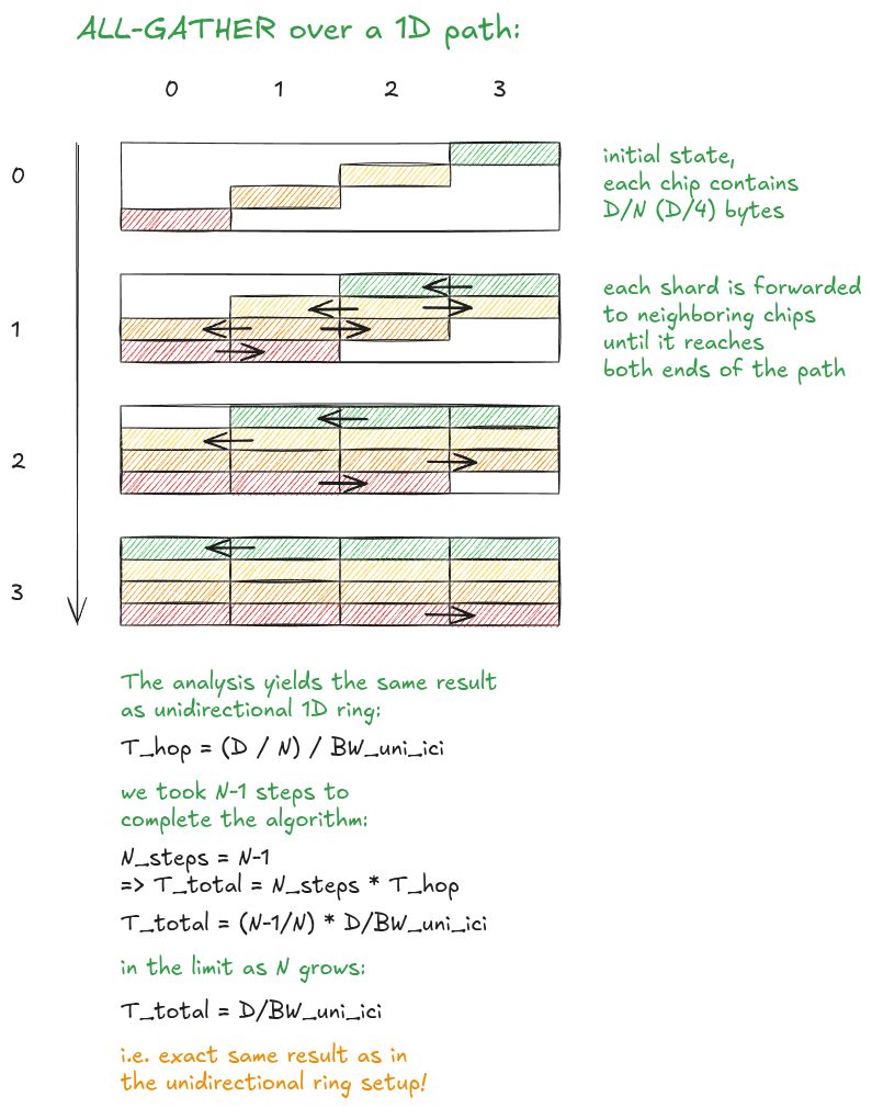
Figure 14: All Gather - chain/path
Finally, sometimes we have an array that is sharded across both axes of the TPU slice, and we want to perform a 2D All-Gather.
最后,有时候我们的数组是跨 TPU slice 的两个轴切分的,这时我们要做 2D All-Gather。
In that case, we can use all 4 neighboring ICI links, which gives us a 2× speedup compared to using only a single axis!
这种情况下,我们可以用上全部 4 条相邻的 ICI 链路,相比只用单轴能拿到 2× 的加速!
Let’s build intuition for why. Assume a hypothetical 4 × 4 slice with wraparound links along both axes, so both rows and columns form rings:
我们来建立直觉。假设一个 4 × 4 的 slice,两个轴都有环绕链路,于是行和列都构成 ring:
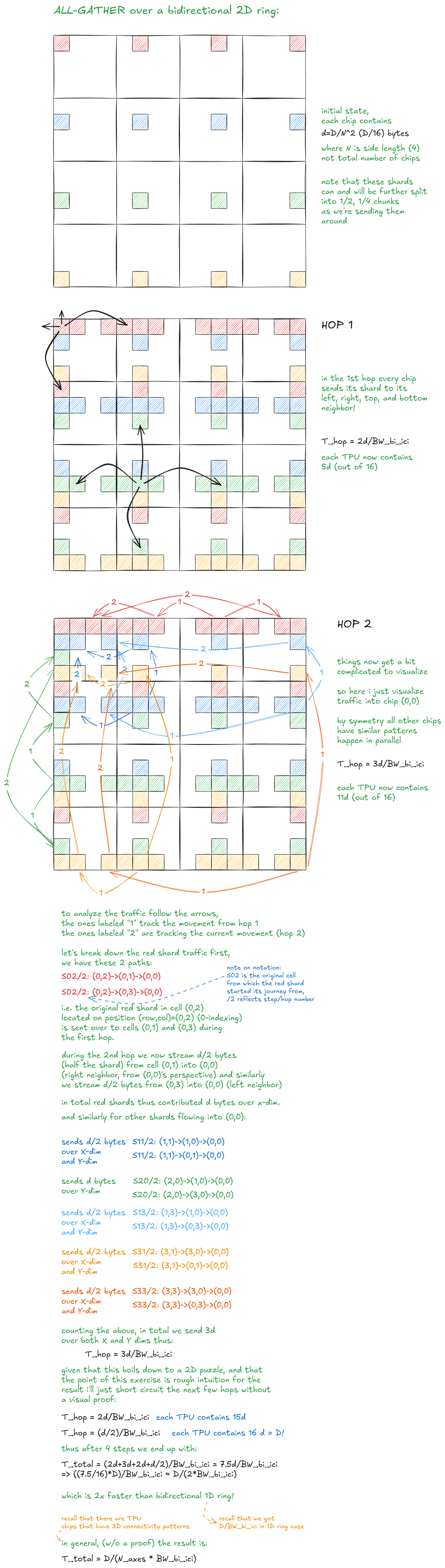
Figure 15: All Gather over a bidirectional 2D ring
That’s a wrap for All-Gather.
All-Gather 就到这里。
Next, let’s look at its dual, Reduce-Scatter, and then use it to build All-Reduce.
接下来看它的对偶——Reduce-Scatter,然后用它搭出 All-Reduce。
As before, let’s start with a motivating example:
和前面一样,先看一个动机例子:
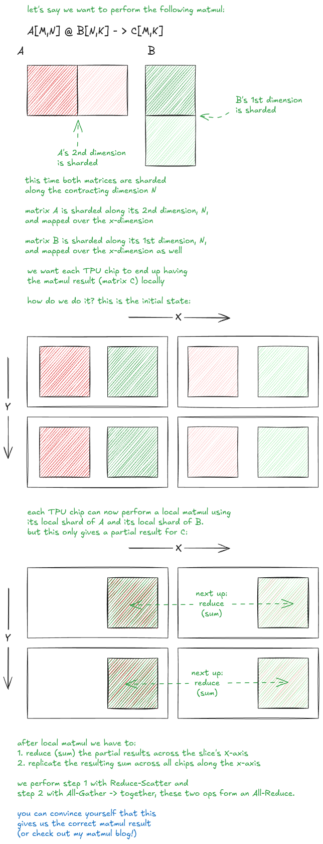
Figure 16: Reduce-Scatter motivation
So how do we efficiently implement Reduce-Scatter?
那我们怎么高效实现 Reduce-Scatter?
It turns out to be very similar to All-Gather. In fact, you can think of it as All-Gather’s dual: the communication schedule is very similar, but instead of copying shards as they move, we reduce them as they move.
它其实和 All-Gather 非常像。事实上,你可以把它看成 All-Gather 的对偶:通信时序几乎一样,只不过分片在流动过程中不是被复制,而是被规约(reduce)。
Because the communication pattern is almost identical, the throughput-bound time complexity is the same:
正因为通信模式几乎相同,它在 throughput-bound 下的时间复杂度也一样:
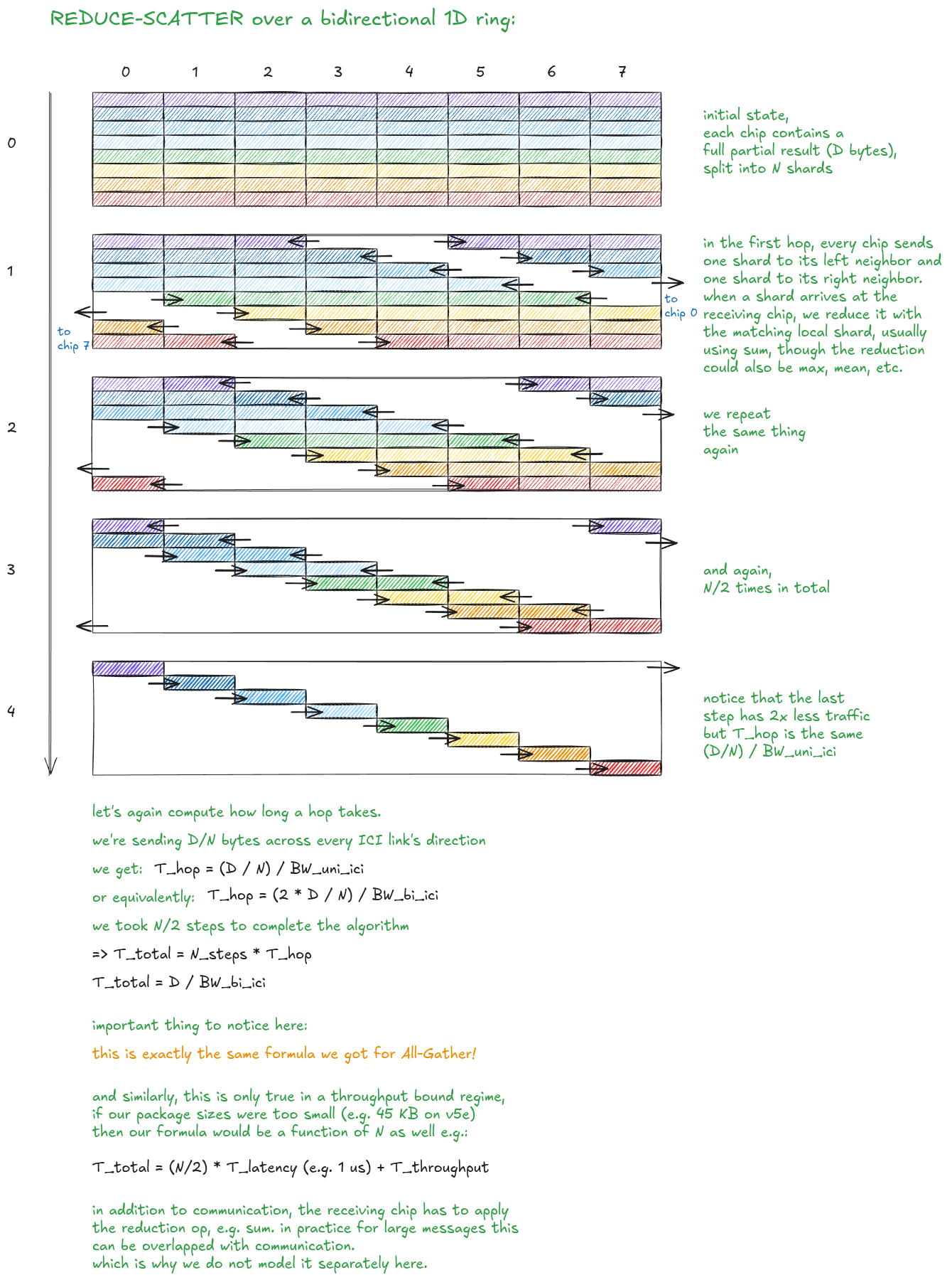
Figure 17: Reduce-Scatter over a bidirectional 1D ring
💡 Side note: All-Gather/Reduce-Scatter duality:
There is a useful duality between All-Gather and Reduce-Scatter. For many sharding patterns, if the forward pass uses All-Gather, the backward pass uses Reduce-Scatter. Conversely, if the forward pass uses Reduce-Scatter, the backward pass uses All-Gather. This is worth being aware of, but since the focus of this post is the mechanics of collective operations, I won’t expand on it further here.
💡 补充:All-Gather/Reduce-Scatter 的对偶性:
All-Gather 和 Reduce-Scatter 之间存在一个有用的对偶关系。对许多切分方式来说,如果前向传播用的是 All-Gather,那么反向传播用的就是 Reduce-Scatter;反过来,如果前向用的是 Reduce-Scatter,反向用的就是 All-Gather。这一点值得留意,不过本文的重点是集合通信的机制,这里就不展开了。
Continuing the motivating example above, we can now see how to build All-Reduce from Reduce-Scatter followed by All-Gather:
接着上面的动机例子,我们现在可以看到如何用 Reduce-Scatter 加 All-Gather 搭出 All-Reduce:
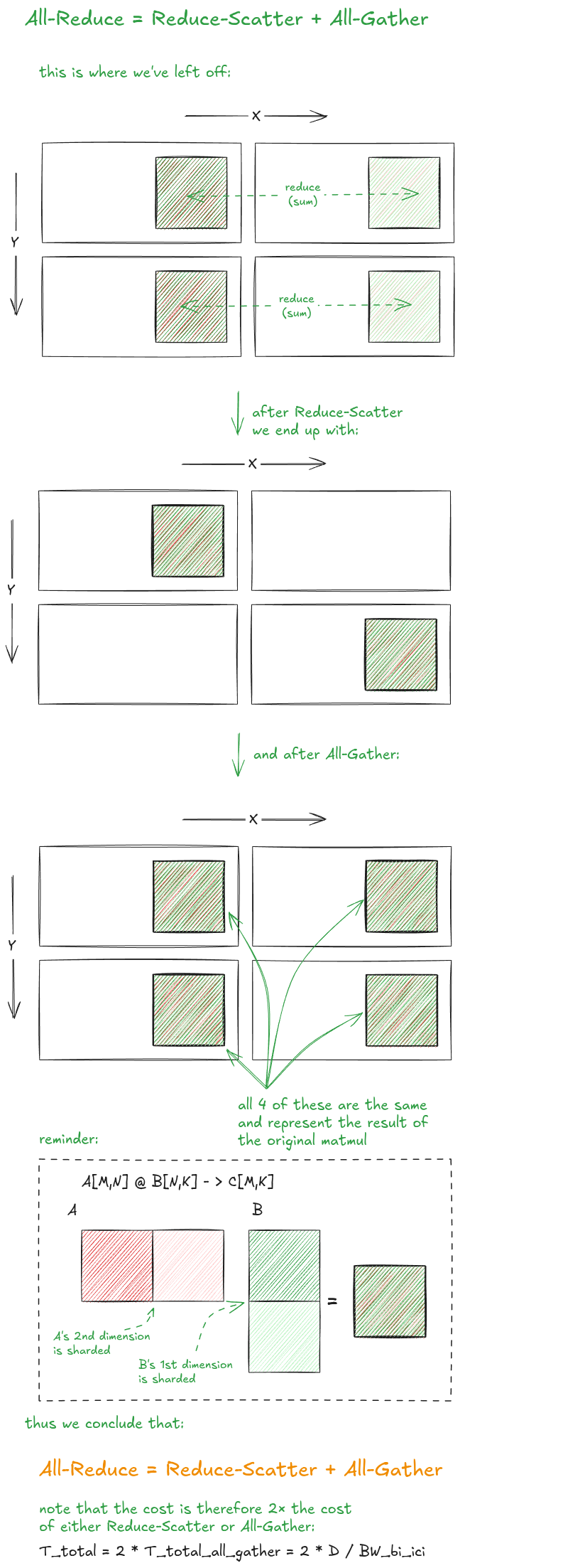
Figure 18: All-Reduce over a bidirectional 1D ring
For consistency’s sake let’s also cover Reduce-Scatter over a hypothetical (because we’d need 16 TPUs not 4 to get a ring on v5e) unidirectional 1D ring:
为了一致性,我们也把单向 1D ring 上的 Reduce-Scatter 过一遍(之所以说“假设”,是因为在 v5e 上要拿到 ring 需要 16 颗 TPU 而不是 4 颗):
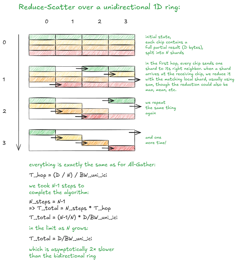
Figure 19: Reduce-Scatter over a unidirectional 1D ring
Finally, if we take a TPU slice without wraparound links, for example, a 4 × 4 v5e slice, then there is no ring structure along that axis. In that case, we fall back to Reduce-Scatter over a 1D path / chain:
最后,如果我们取一个没有环绕链路的 TPU slice,比如 4 × 4 的 v5e slice,那么这个轴上没有 ring 结构。这时 Reduce-Scatter 就退化成沿 1D path / chain 进行:
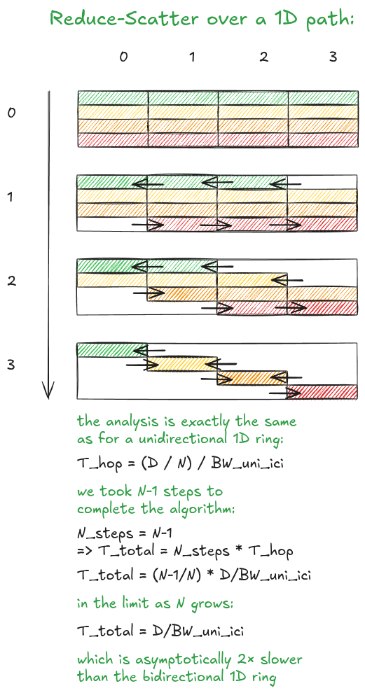
Figure 20: Reduce-Scatter - chain/path
As with All-Gather, if the data is sharded across multiple topology axes, we can use more ICI links in parallel. In the throughput-bound regime, the total time scales roughly inversely with the number of topology axes we use.
和 All-Gather 一样,如果数据跨多个拓扑轴切分,我们可以并行用上更多 ICI 链路。在 throughput-bound 的 regime 下,总时间大致与所用拓扑轴的数量成反比。
That wraps up Reduce-Scatter and All-Reduce!
Reduce-Scatter 和 All-Reduce 就讲完了!
Let’s now look at the final primitive: All-to-All.
现在来看最后一个原语:All-to-All。
A canonical place where All-to-All shows up is in MoE (Mixture-of-Experts) models.
All-to-All 最典型的出场场景是 MoE(Mixture-of-Experts)模型。
💡 MoE simplified:
For simplicity, assume top-1 routing and one expert per chip.
💡 MoE 简化版:
为简单起见,假设是 top-1 路由,且每颗芯片放一个 expert。
In an MoE layer, each token is assigned to one expert by the router. You can think of the router as attaching a destination expert ID to each token.
在 MoE 层里,每个 token 由 router 分配给一个 expert。你可以把 router 理解为给每个 token 贴上一个目标 expert ID。
Assume that the Expert 0 lives on TPU 0, Expert 1 lives on TPU 1, and so on. Then the expert ID tells us which TPU chip the token needs to be sent to.
假设 Expert 0 住在 TPU 0 上,Expert 1 住在 TPU 1 上,以此类推。那么 expert ID 就告诉我们这个 token 需要被送到哪颗 TPU 芯片。
So each chip starts with a local batch of tokens, but those tokens may be destined for many different experts on many different chips.
于是每颗芯片手上都有一批本地 token,但这些 token 可能需要发往许多不同芯片上的许多不同 expert。
All-to-All is the collective that performs this exchange: every chip sends its tokens for Expert 0 to TPU 0, the tokens for Expert 1 to TPU 1, and so on.
All-to-All 就是完成这次交换的集合通信:每颗芯片把属于 Expert 0 的 token 发给 TPU 0,把属于 Expert 1 的 token 发给 TPU 1,依此类推。
In other words, All-to-All is a kind of distributed transpose: we start grouped by source chip, and after the collective we are grouped by destination expert.
换句话说,All-to-All 是一种分布式的转置:开始时按源芯片分组,集合通信结束后则按目标 expert 分组。
For the diagrams below, we’ll assume a perfectly balanced routing pattern: each chip has the same amount of data destined for every other chip. Real MoE routing can be imbalanced, but the balanced case gives us the cleanest mental model for understanding the All-to-All primitive.
下面几张图里,我们假设路由是完全均衡的:每颗芯片发往其他任意芯片的数据量都相同。真实的 MoE 路由可能不均衡,但均衡情形能给出理解 All-to-All 原语最清晰的心智模型。
Here is how we do All-to-All over a bidirectional 1D ring:
这是双向 1D ring 上做 All-to-All 的方式:
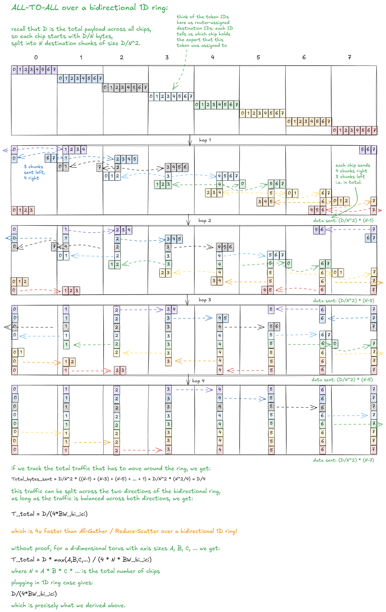
Figure 21: All-to-all over a bidirectional 1D ring
Here is All-to-All over a unidirectional 1D ring:
这是单向 1D ring 上的 All-to-All:
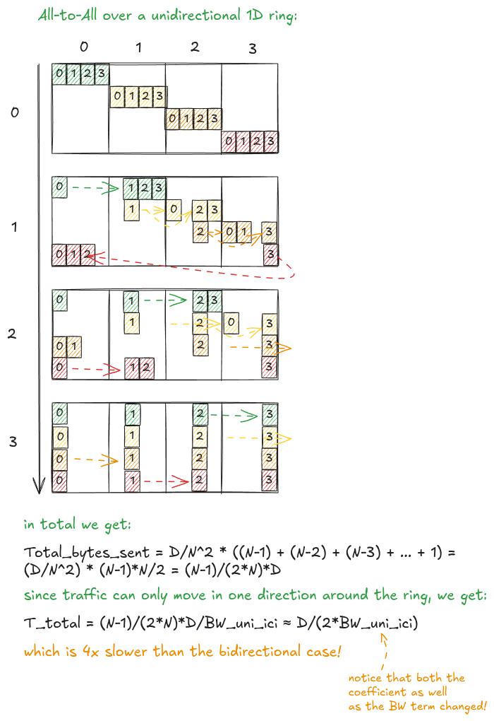
Figure 22: All-to-All over a unidirectional 1D ring
Same story as before: without wraparound links, the ring becomes a path. So on a 4 × 4 v5e slice, All-to-All falls back to a 1D path / chain algorithm:
和之前一样:没有环绕链路时,ring 就变成了 path。所以在 4 × 4 的 v5e slice 上,All-to-All 退化成 1D path / chain 算法:
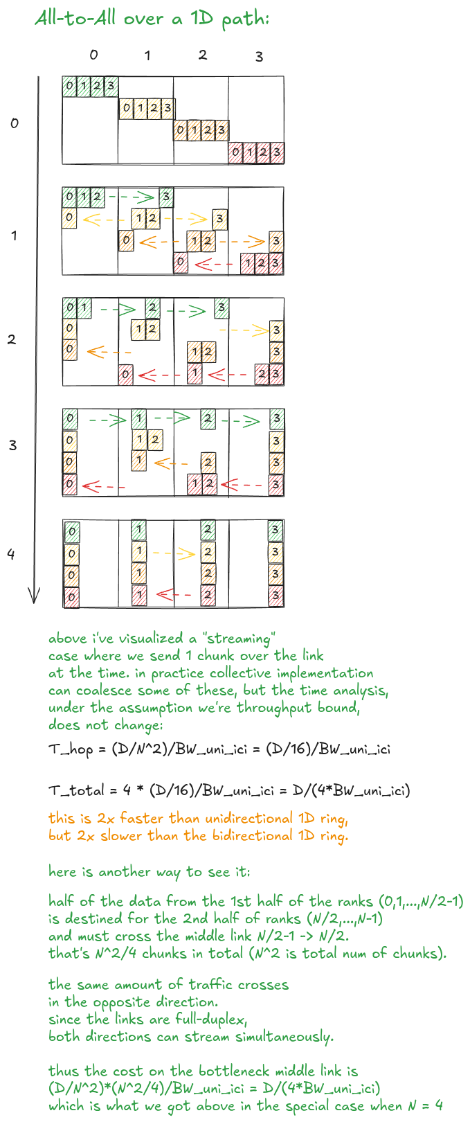
Figure 23: All-to-all - chain/path
To wrap up the TPU part of the blog, let’s summarize the throughput-bound communication-time results:
TPU 这部分收尾之前,我们把 throughput-bound 下的通信时间结论汇总一下:
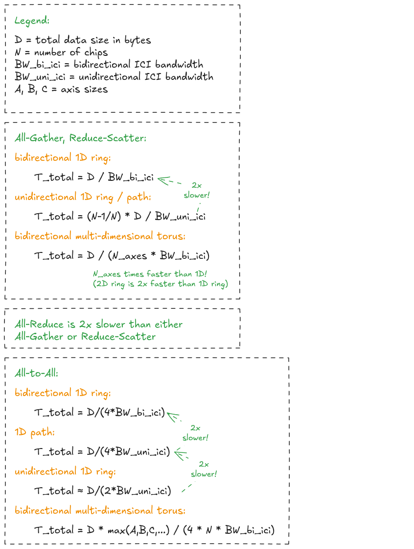
Figure 24: Summary of TPU collective communication costs
Next up, NVIDIA GPUs!
接下来,轮到 NVIDIA GPU 了!
NVIDIA GPU 集群拓扑:Node、Scalable Unit、Fat Tree
In contrast to TPU clusters, which use nearest-neighbor torus connectivity, GPU clusters are usually organized as hierarchical switching networks.
TPU 集群用的是最近邻的 torus 连接,与此不同,GPU 集群通常组织成分层交换网络。
In this post, I’ll focus on the NVIDIA DGX H100 SuperPod reference architecture -> a 1024-GPU cluster organized as a “fat tree”. I’ll explain what “fat tree” means in a moment.
本文聚焦 NVIDIA DGX H100 SuperPod 的参考架构 —— 一个组织成 “fat tree” 的 1024 卡集群。稍后我会解释 “fat tree” 是什么意思。
I’ll focus solely on the compute fabric: the network used for GPU-to-GPU communication during distributed training. I’ll ignore the storage fabric used for checkpoints, weights, logs, and datasets; UFM for InfiniBand monitoring/management; and the in-band / out-of-band management fabrics used for cluster operations. i.e. the other subsystems that make up a functional NVIDIA cluster.
我只讲计算网络:也就是分布式训练里用于 GPU 之间通信的那张网。存储网络(用于 checkpoint、权重、日志和数据集)、用于 InfiniBand 监控管理的 UFM、以及用于集群运维的带内/带外管理网络都不讲。也就是说,一个能跑起来的 NVIDIA 集群里其他那些子系统,这里都略过。
Here are the basics.
先说最基础的。
The first organizing unit is the node. In this section, I’ll use “node” to mean the local NVLink / NVSwitch scale-up domain. For example, a DGX H100 node has 8 H100 GPUs connected through NVLink fabric (and e.g. GB200 NVL72 has 72 GPUs).
第一个组织单元是 node(节点)。本节里,“node” 指的是本地 NVLink / NVSwitch 的 scale-up 域。比如一个 DGX H100 节点有 8 张 H100 GPU 通过 NVLink fabric 相连(再比如 GB200 NVL72 有 72 张 GPU)。
💡 Terminology note:
NVSwitch / NVLink fabric is just NVIDIA’s terminology for high bandwidth switches / interconnects that connect the GPUs.
💡 术语说明:
NVSwitch / NVLink fabric 只是 NVIDIA 对连接 GPU 的高带宽交换机 / 互联的叫法。
Inside the node, GPUs are effectively connected all-to-all through the NVSwitch fabric: every GPU can reach every other GPU in one NVSwitch hop.
在节点内部,GPU 之间通过 NVSwitch fabric 事实上是全连接的:每张 GPU 都能一跳 NVSwitch 到达其他任意一张 GPU。
Nodes are then connected together through InfiniBand (IB), which forms the scale-out network. In the DGX H100 SuperPod reference architecture, 32 nodes form a Scalable Unit (SU), connected through InfiniBand leaf switches. Multiple SUs are then connected through higher-level spine switches.
节点之间则通过 InfiniBand(IB)相连,构成 scale-out 网络。在 DGX H100 SuperPod 参考架构里,32 个节点构成一个 Scalable Unit(SU),通过 InfiniBand 的 leaf 交换机相连。多个 SU 再通过更高层的 spine 交换机相连。
This hierarchy forms a fat tree.
这个层次结构构成一棵 fat tree。
This architecture is called a “fat tree” because the tree gets “fatter” toward the root: upper levels have more aggregate bandwidth, so traffic from many nodes does not collapse into a narrow bottleneck.
之所以叫 “fat tree”,是因为这棵树越往根部越“粗”:上层拥有更大的聚合带宽,因此来自众多节点的流量不会塌缩进一个狭窄的瓶颈。
A full fat tree is the non-oversubscribed / special version of this idea. At each level, the uplink bandwidth matches the downstream injection bandwidth (this will become much clearer in the figure below).
full fat tree 是这一思路的非超配(non-oversubscribed)版本。在每一层,上行带宽都与下行的注入带宽相匹配(看下面那张图会更清楚)。
💡 Terminology note:
Oversubscription means the downstream devices can inject more traffic than the upstream links can carry. For example, if a group of nodes can inject 12.8 TB/s into the leaf layer, but the leaf switches only have 6.4 TB/s of uplink bandwidth to the spine layer, then the fabric is 2 oversubscribed. A full fat tree is non-oversubscribed: at each level, upstream bandwidth matches downstream injection bandwidth.
💡 术语说明:
超配(oversubscription)指的是下行设备能注入的流量超过上行链路能承载的量。比如一组节点能以 12.8 TB/s 注入 leaf 层,而 leaf 交换机到 spine 层只有 6.4 TB/s 的上行带宽,那么这张 fabric 就是 2 超配。full fat tree 是非超配的:每一层的上行带宽都等于下行的注入带宽。
The key consequence of having a full fat tree is full bisection bandwidth.
full fat tree 的关键推论是全双分带宽(full bisection bandwidth)。
Bisection bandwidth is the bandwidth available across an equal split of the cluster. So if we split a 128-node cluster into two groups of 64 nodes, each side can communicate with the other at its full aggregate injection bandwidth!
**Bisection bandwidth(二分带宽)**是指把集群对半切开时,跨越这条割的可用带宽。所以如果我们把一个 128 节点的集群切成两组各 64 节点,每一边都能以自己完整的聚合注入带宽与另一边通信!
More generally, for any partition, the cross-partition bandwidth is limited by the number of nodes on the smaller side of the split.
更一般地,对任意切分,跨切分带宽受限于切分中较小一侧的节点数。
For example, each DGX H100 node has 8 × 50 GB/s links into the IB compute fabric, giving it 400 GB/s of unidirectional injection bandwidth. In a full fat tree, any group of N nodes can communicate across a partition at N × 400 GB/s in one direction, assuming N is the smaller side of the split.
比如,每个 DGX H100 节点有 8 条 × 50 GB/s 的链路接入 IB 计算网络,也就是 400 GB/s 的单向注入带宽。在 full fat tree 里,任意 N 个节点组成的一组,只要 N 是切分中较小的一侧,就能以 N × 400 GB/s 的单向速率跨切分通信。
Inside a node, the same idea applies to the local NVLink/NVSwitch fabric. If we split the 8 GPUs into two groups of 4, one side can send to the other at:
在节点内部,同样的思路适用于本地 NVLink/NVSwitch fabric。如果我们把 8 张 GPU 切成两组各 4 张,一侧能以如下速率发给另一侧:
4 × 450 GB/s = 1.8 TB/s (which is the max bandwidth for those 4 GPUs!)
4 × 450 GB/s = 1.8 TB/s(这已经是那 4 张 GPU 的最大带宽了!)
Since the fabric is full-duplex, the bidirectional bisection bandwidth is:
由于 fabric 是全双工的,双向二分带宽是:
2 × 1.8 TB/s = 3.6 TB/s
At the Scalable Unit level, we have 32 nodes. For a true bisection, we split the SU into two groups of 16 nodes. One side can send to the other at:
在 Scalable Unit 这一层,我们有 32 个节点。真正对半分的话,把 SU 切成两组各 16 个节点。一侧能以如下速率发给另一侧:
16 × 400 GB/s = 6.4 TB/s (bidirectional bisection bw -> 12.8 TB/s)
16 × 400 GB/s = 6.4 TB/s(双向二分带宽 -> 12.8 TB/s)
Finally, if we split the cluster into 64 nodes and 64 nodes, one side can send to the other at:
最后,如果把集群切成 64 节点和 64 节点,一侧能以如下速率发给另一侧:
64 × 400 GB/s = 25.6 TB/s (bidirectional bisection bw -> 51.2 TB/s)
64 × 400 GB/s = 25.6 TB/s(双向二分带宽 -> 51.2 TB/s)
For an uneven partition, say 88 nodes on one side and 40 nodes on the other, the cross-partition bandwidth is limited by the smaller side:
对于不均匀的切分,比如一侧 88 个节点、另一侧 40 个节点,跨切分带宽受限于较小的一侧:
40 × 400 GB/s = 16 TB/s
With that mental model, let’s analyze the DGX H100 reference architecture in more detail. Feel free to zoom in:
有了这个心智模型,我们更细致地分析一下 DGX H100 参考架构。欢迎放大看:
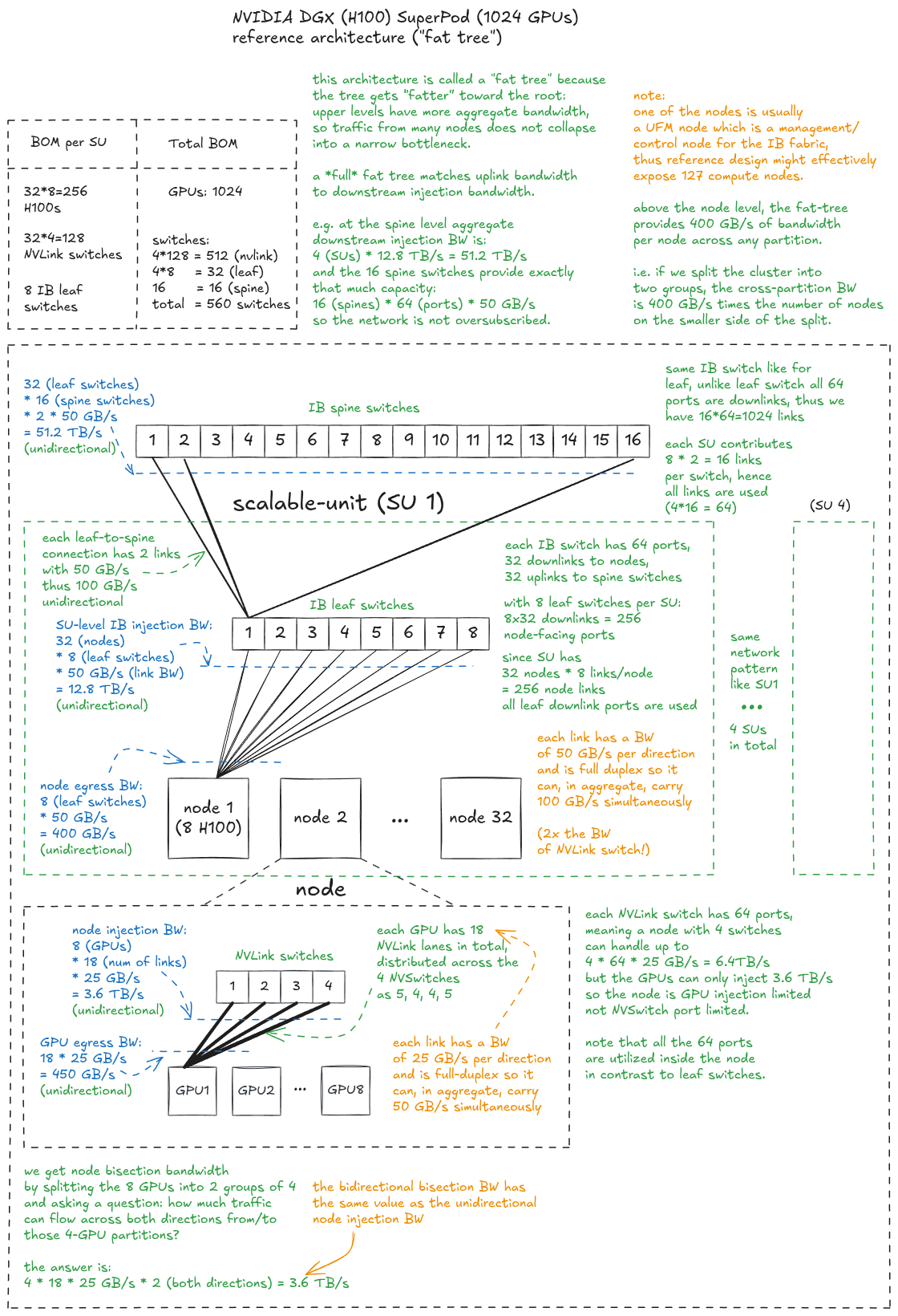
Figure 25: NVIDIA DGX (H100) SuperPod (1024 GPUs) reference architecture
With the GPU cluster topology in mind, we’re ready to shift our focus to collective operations.
GPU 集群拓扑清楚了,我们可以把注意力转到集合通信操作上。
In the intra-node setting (i.e. within a single GPU node), the collective algorithms look similar to the TPU case because they both operate on an abstract ring structure, but the underlying topology is different.
在节点内(也就是单张 GPU 节点内部)的场景里,集合通信算法看起来和 TPU 那边很像,因为两者都跑在一个抽象的 ring 结构上,但底层拓扑不同。
On TPUs, the ring is a physical path through nearest-neighbor ICI links. On GPUs, the ring is a logical ordering chosen over the NVSwitch fabric.
在 TPU 上,ring 是穿过最近邻 ICI 链路的一条物理路径。在 GPU 上,ring 则是在 NVSwitch fabric 之上选出来的一个逻辑顺序。
The NVSwitch fabric gives us effective all-to-all connectivity between GPUs, and the collective algorithm chooses a ring on top of that connectivity pattern.
NVSwitch fabric 给了我们 GPU 之间事实上的全连接,集合通信算法就在这个连接模式之上挑选一个 ring。
Let’s break this down:
我们来拆解一下:
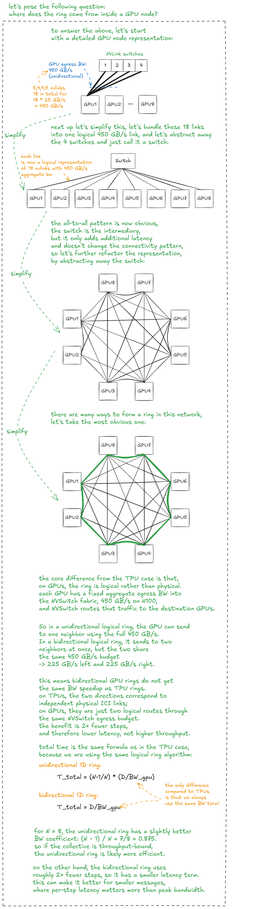
Figure 26: Constructing a logical ring inside a GPU node
As we already know, All-Reduce can be implemented as Reduce-Scatter followed by All-Gather, so without special hardware support its communication cost is roughly 2× higher than either primitive alone.
如我们所知,All-Reduce 可以用 Reduce-Scatter 加 All-Gather 实现,所以在没有特殊硬件支持时,它的通信开销大约是单独任一个原语的 2 倍。
NVIDIA GPU switches (both NVSwitch and IB switches) have an important optimization called SHARP, an in-network reduction compute unit. Normally, a switch just routes data between GPUs. With SHARP, the switch can also perform the reduction operation itself. For example, instead of GPUs exchanging partial sums and reducing them locally, the GPUs send their partial values into the switch, the switch sums them, and the reduced result is sent back.
NVIDIA 的 GPU 交换机(NVSwitch 和 IB 交换机都有)有一个重要优化叫 SHARP,即网络内规约计算单元。通常交换机只是在 GPU 之间转发数据;有了 SHARP,交换机自己也能做规约运算。比如,GPU 不必互相交换部分和再在本地规约,而是把各自的部分值发进交换机,交换机求和,再把规约后的结果发回来。
So instead of spending SM cycles and HBM bandwidth on a largely memory-bound All-Reduce, the network performs the reduction in flight, leaving the GPUs free for useful computation.
于是,不必再为一个大体上 memory-bound 的 All-Reduce 消耗 SM 周期和 HBM 带宽,网络在传输途中就把规约做掉了,把 GPU 留给真正有用的计算。
💡 SHARP’s FLOPs/s:
As a reference point, the NVLink 4 NVSwitch (found in H100 nodes) SHARP has 400 GFLOP/s of FP32 reduction throughput [4].
💡 SHARP 的 FLOPs/s:
作为参考,H100 节点里的 NVLink 4 NVSwitch SHARP 有 400 GFLOP/s 的 FP32 规约吞吐 [4]。
SHARP can theoretically make All-Reduce close to 2× faster! In the limit where N, the number of GPUs in the node, grows large, the improvement approaches 2×; for 8-GPU nodes, the ideal improvement is closer to 1.75×.
理论上 SHARP 能让 All-Reduce 快接近 2×!在节点内 GPU 数量 N 趋于无穷的极限下,提升趋近 2×;对 8 卡节点,理想提升接近 1.75×。
So how does SHARP work?
那 SHARP 是怎么工作的?
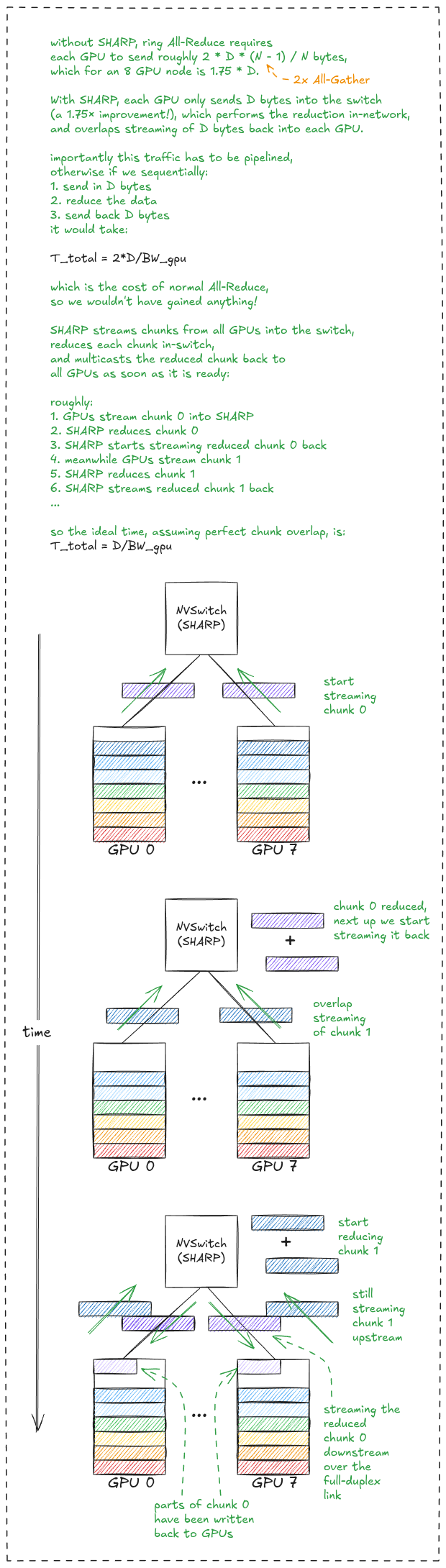
Figure 27: SHARP - in-network reduction compute unit
💡 Theory vs practice:
Empirically, All-Reduce on GPUs can require very large messages to approach peak BW. In older NCCL measurements[5] on an 8×H100 node, performance was still ramping even at multi-GB message sizes, and bandwidth dropped noticeably once the message size fell below roughly 100 MB. This is one practical difference from TPUs, which tend to reach near-peak collective BW at much smaller message sizes (~10 MBs).
Even with SHARP enabled for All-Reduce, we should still account for overhead: the reduce + multicast pipeline will not overlap perfectly in practice. In practice speedups from SHARP are only about 30%[5][6]! Always run microbenchmarks on your concrete cluster setup.
💡 理论与实践:
经验上,GPU 上的 All-Reduce 需要非常大的消息才能逼近峰值带宽。在 8×H100 节点上的早期 NCCL 测量[5]中,即使消息到了多 GB 量级,性能仍在爬升;而一旦消息小于大约 100 MB,带宽就明显下降。这是和 TPU 的一个实际差异:TPU 往往在小得多的消息(约 10 MB)上就能接近集合通信峰值带宽。
即便为 All-Reduce 打开了 SHARP,也仍然要算上开销:规约 + 组播流水线在实践中不会完美重叠。实际中 SHARP 带来的加速只有大约 30%[5][6]!永远要在你自己的具体集群上跑 microbenchmark。
💡 Additional SHARP context:
NVLink SHARP is not limited to reductions, it also accelerates the All-Gather phase through hardware multicast. A memory region can be registered as a multicast target for a group of GPUs. After that, a normal CUDA store to the multicast address is replicated by the NVSwitch fabric to every GPU in the group - the kernel itself does not need a special multicast instruction.
One inefficiency is that the multicast includes the source GPU as well, even though it already has the data! (wasting 1/8th of BW in an H100 node).
💡 SHARP 的补充背景:
NVLink SHARP 不只限于规约,它还通过硬件组播加速 All-Gather 阶段。一块内存区域可以注册为一组 GPU 的组播目标。之后,对这个组播地址做一次普通的 CUDA store,就会被 NVSwitch fabric 复制到组内的每张 GPU —— kernel 本身不需要任何特殊的组播指令。
一个低效之处在于:组播也会发给源 GPU,尽管它本来就有这份数据!(在 H100 节点里浪费了 1/8 的带宽)。
Inside an NVSwitch node, balanced All-to-All can require roughly 2× less communication time than on a bidirectional 1D torus ring (assuming equal bandwidths), because every GPU can send directly to every destination GPU:
在 NVSwitch 节点内部,均衡的 All-to-All 所需通信时间大约比双向 1D torus ring 少 2 倍(假设带宽相同),因为每张 GPU 都能直接发给任意目标 GPU:
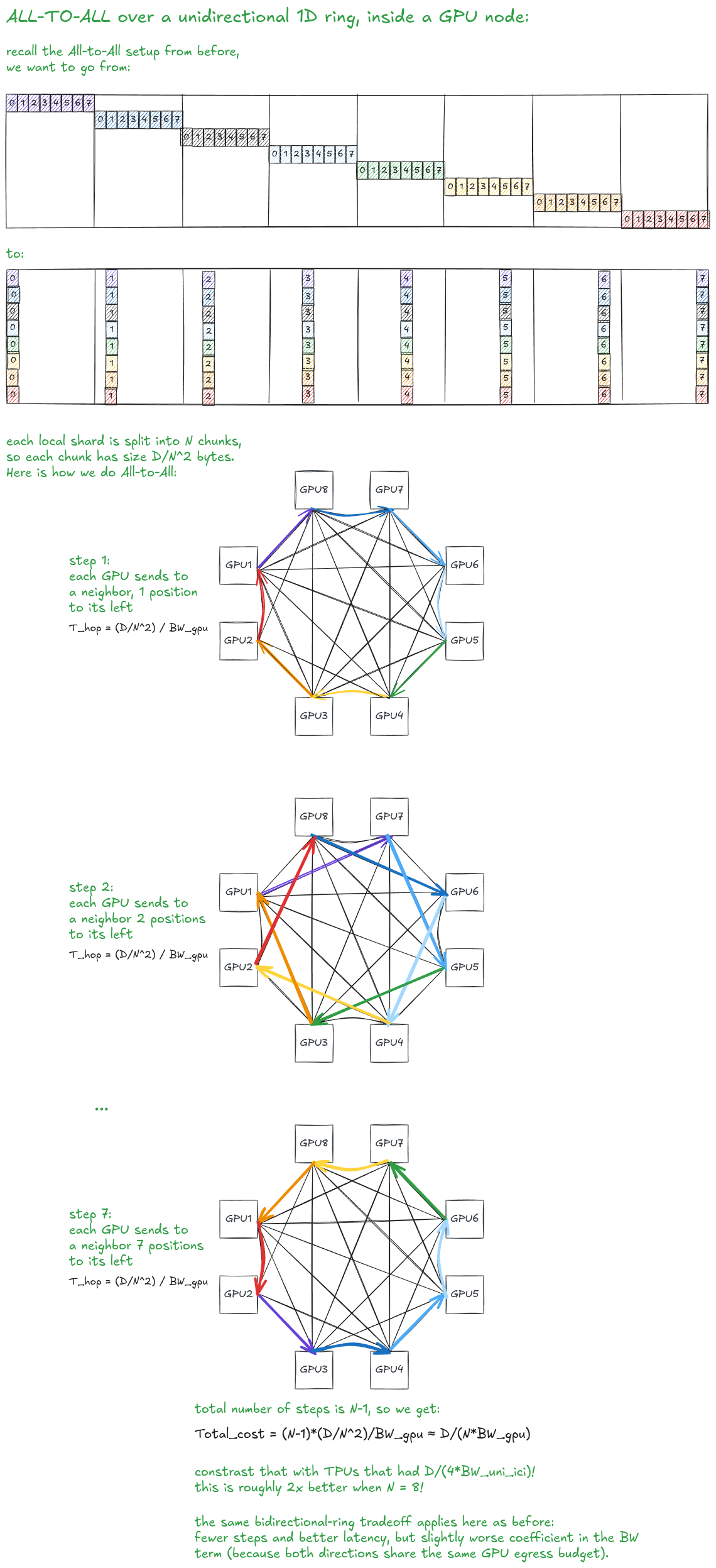
Figure 28: Dense All-to-All over a logical unidirectional ring inside an 8-GPU node
💡 All-to-All on NVL72:
The dense, balanced All-to-All model is a reasonable simplification for an 8-GPU H100 node, but it becomes less representative on systems such as GB200 NVL72. In an MoE inference workload with 72 GPUs and only eight experts selected per token, each token needs to reach only about 8/72≈11% of the GPUs. Communication therefore becomes sparse and ragged rather than a uniform All-to-All: the router first determines each token’s destination experts, and the system sends that token only to the GPUs hosting those experts.
💡 NVL72 上的 All-to-All:
稠密、均衡的 All-to-All 模型对 8 卡 H100 节点是个合理的简化,但在 GB200 NVL72 这类系统上就不太有代表性了。在 72 张 GPU、每个 token 只选 8 个 expert 的 MoE 推理负载里,每个 token 只需要到达大约 8/72≈11% 的 GPU。于是通信变得稀疏而参差,不再是均匀的 All-to-All:router 先确定每个 token 的目标 expert,系统只把该 token 发给承载这些 expert 的那些 GPU。
Before we move to inter-node collective ops, I want to briefly cover the main idea behind tree-based collectives.
在转向节点间集合通信之前,我想简单讲讲 tree 类集合通信的核心思路。
The main idea is to pair GPUs in rounds, doubling the amount of data each GPU has after every round. This gives us log₂(N) communication steps instead of N - 1.
核心思路是:分轮次把 GPU 两两配对,每一轮之后每张 GPU 手上的数据量翻倍。这样通信步数从 N - 1 变成 log₂(N)。
Here is tree-based All-Gather, implemented as recursive doubling:
这是 tree 版 All-Gather,用递归倍增(recursive doubling)实现:
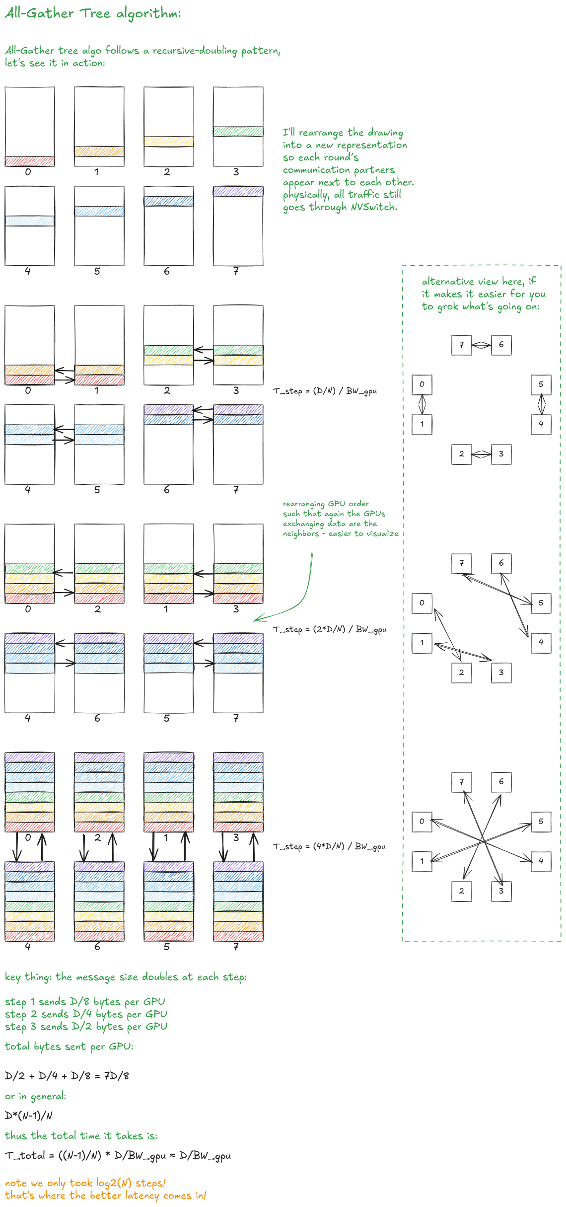
Figure 29: Tree All-Gather
A few notes on tree vs. ring algorithms.
关于 tree 与 ring 算法,有几点要说。
Both ring and tree algorithms have step dependencies, but rings are usually easier to pipeline. In a ring, many chunks can be streamed continuously around the ring, keeping links busy. Recursive doubling can have lower latency complexity, but for large messages it may achieve lower effective bandwidth than ring because it is less pipeline-friendly.
ring 和 tree 算法都存在步与步之间的依赖,但 ring 通常更容易流水化。在 ring 里,许多分块可以绕着环连续不断地流动,让链路一直忙起来。递归倍增的延迟复杂度可能更低,但对大消息,它的有效带宽可能低于 ring,因为它不太利于流水线。
In the ideal bandwidth model, the byte cost is the same (as you can see in the figure above), but tree-style algorithms reduce the number of communication rounds from N - 1 to log₂(N). In practice, rings often achieve higher effective bandwidth on large tensors, so libraries like NCCL choose between ring, tree, and hybrid algorithms based on message size and topology.
在理想带宽模型下,字节开销是一样的(如上图所示),但 tree 风格算法把通信轮数从 N - 1 降到 log₂(N)。实践中,ring 在大张量上往往能取得更高的有效带宽,所以 NCCL 这类库会根据消息大小和拓扑在 ring、tree 和混合算法之间做选择。
For completeness, here is Reduce-Scatter via recursive halving:
为完整起见,这里是基于递归折半(recursive halving)的 Reduce-Scatter:
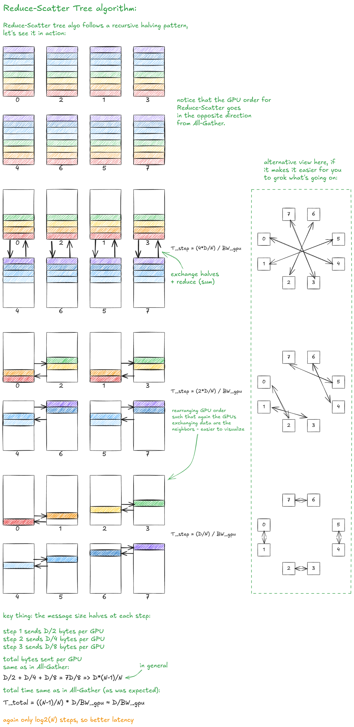
Figure 30: Tree Reduce-Scatter
Next, let’s see what changes when we move outside a single GPU node and into the inter-node setting.
接下来看看当我们走出单个 GPU 节点、进入节点间场景时,会有什么变化。
跨节点的 GPU 集合通信:InfiniBand 上的分层算法
The low-level details of algorithms become more involved due to pipelining over multiple hierarchy levels (node-level, SU-level, spine-level).
算法的底层细节会变得更复杂,因为要在多个层级(节点级、SU 级、spine 级)上做流水线。
A good mental model is to imagine running one inter-node ring over every node in the cluster (this we can do thanks to the non-oversubscribed/full fat tree).
一个不错的心智模型是:想象在集群里每个节点上都跑一条节点间的 ring(之所以能做到,靠的就是非超配的 full fat tree)。
For large messages, a good first-order approximation for All-Gather or Reduce-Scatter is therefore (where D is the tensor size in bytes):
因此,对大消息,All-Gather 或 Reduce-Scatter 的一阶近似是(其中 D 是张量大小,单位字节):
T_total ≈ D / BW_node = D / 400e9
A slightly more accurate model also accounts for the intra-node stage. In hierarchical collectives, we usually have both scale-out traffic over IB and local traffic over NVLink/NVSwitch, and these stages can often be pipelined. So the total time is closer to the slower of the two terms:
再精确一点的模型会把节点内那一段也算进去。在分层集合通信里,我们通常同时有跨 IB 的 scale-out 流量和走 NVLink/NVSwitch 的本地流量,而这两段常常可以流水起来。于是总时间更接近两项中较慢的那个:
T_total ≈ max(D/BW_gpu, D/BW_node)
Let’s start with the first cross-node collective - All-Gather:
先看第一个跨节点集合通信 —— All-Gather:
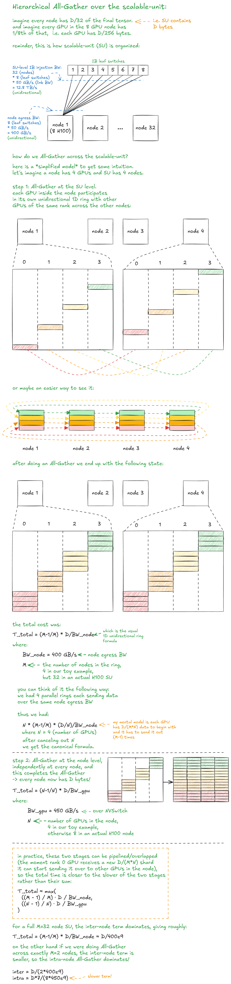
Figure 31: Hierarchical All-Gather over the scalable-unit
💡 Why no spine switch?
For these examples, I’m only showing communication within a single SU. Adding the spine fabric doesn’t qualitatively change the algorithm, we’d still run the same kind of hierarchical collective (just across one more level of the topology). It does however complicate visualizations, so I’ll skip doing spine-level collectives.
💡 为什么没有 spine 交换机?
这些例子里,我只展示了单个 SU 内部的通信。加上 spine fabric 并不会在性质上改变算法,我们仍然跑同一种分层集合通信(只是多跨一层拓扑)。但它会让可视化复杂不少,所以 spine 级的集合通信我就跳过了。
💡 Note on rail optimization:
A node’s aggregate inter-node bandwidth is not always fully fungible across all GPUs (like in the simple model I shared above). GPU clusters are often organized into parallel network rails, with particular GPUs having preferred paths into the network. Reaching the full node-level bandwidth therefore depends on rail-aware rank placement and balanced traffic across those paths.
💡 关于 rail 优化:
一个节点的聚合节点间带宽,并不总是能在所有 GPU 之间完全通用(就像我上面给的简化模型那样)。GPU 集群常常被组织成并行的网络 rail,某些 GPU 有进入网络的偏好路径。因此要拿到完整的节点级带宽,取决于能否做到 rail-aware 的 rank 摆放,以及在这些路径之间把流量打均衡。
Next up, let’s look at hierarchical All-Reduce (I’ll skip hierarchical Reduce-Scatter because its structure closely mirrors hierarchical All-Gather):
接下来看分层 All-Reduce(分层 Reduce-Scatter 我就不讲了,因为它的结构和分层 All-Gather 几乎一一对应):
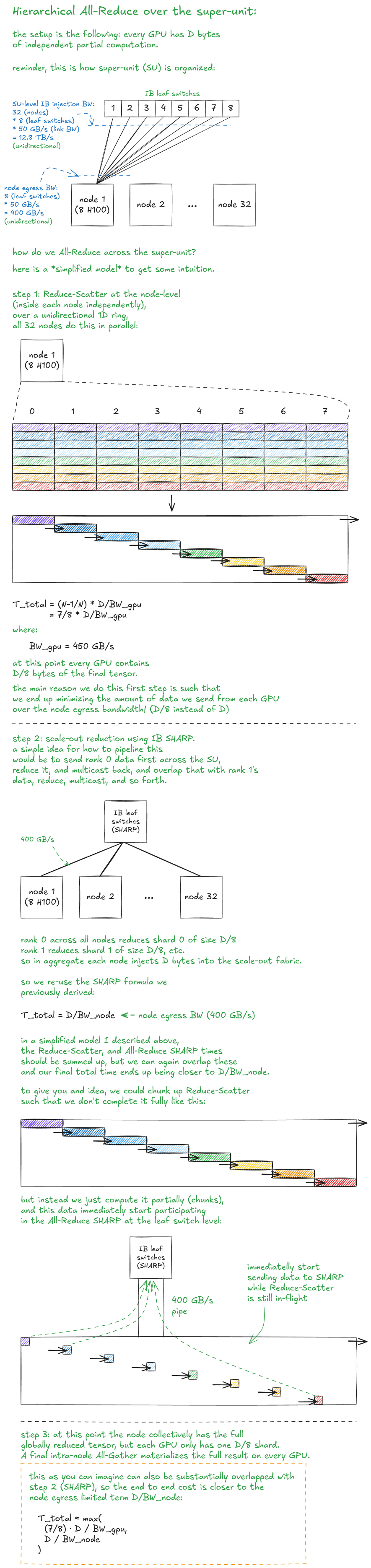
Figure 32: Hierarchical All-Reduce over the scalable-unit
One subtlety: the tensor being All-Reduced may itself be sharded over another parallelism axis.
有一个微妙之处:被 All-Reduce 的那个张量,本身可能还跨另一个并行轴切分着。
For example, in Megatron-style training (tensor/model parallelism), a weight matrix may be sharded over the tensor-parallel axis Y, while its gradients are reduced over the data-parallel axis X.
比如在 Megatron 风格的训练里(张量/模型并行),一个权重矩阵可能沿张量并行轴 Y 切分,而它的梯度要沿数据并行轴 X 做规约。
The All-Reduce is not performed across the tensor-parallel ranks. Those ranks own different shards, so there is nothing elementwise to reduce between them.
这个 All-Reduce 并不是在张量并行的各个 rank 之间做的。那些 rank 各自持有不同的分片,彼此之间没有逐元素可规约的东西。
Instead, for each fixed tensor-parallel shard, we AllReduce across the corresponding data-parallel replicas.
相反,对每一个固定的张量并行分片,我们在对应的数据并行副本之间做 AllReduce。
Let’s work through a concrete example:
我们来走一个具体的例子:
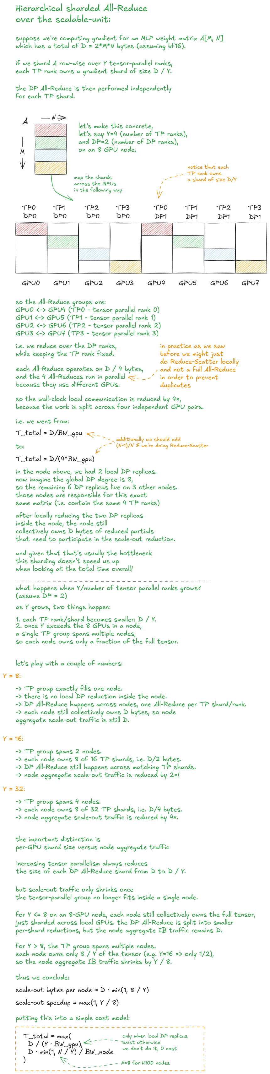
Figure 33: Hierarchical sharded All-Reduce over the scalable-unit
Finally, let’s look at hierarchical All-to-All over a SU.
最后看 SU 上的分层 All-to-All。
Unlike All-Reduce, All-to-All cannot be compressed by doing a local reduction first (each chunk has a specific destination):
与 All-Reduce 不同,All-to-All 没法先做一次本地规约来压缩(每个分块都有明确的目标):
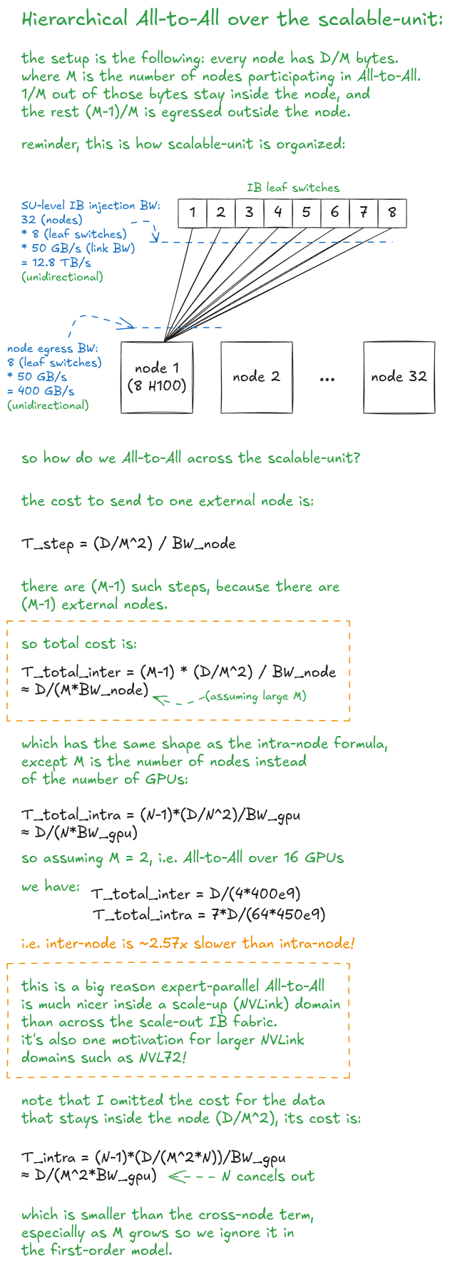
Figure 34: Hierarchical All-to-All over the scalable-unit
As we did in the TPU section, let’s collect the GPU cost models in one place:
和 TPU 那节一样,我们把 GPU 的代价模型汇总在一处:
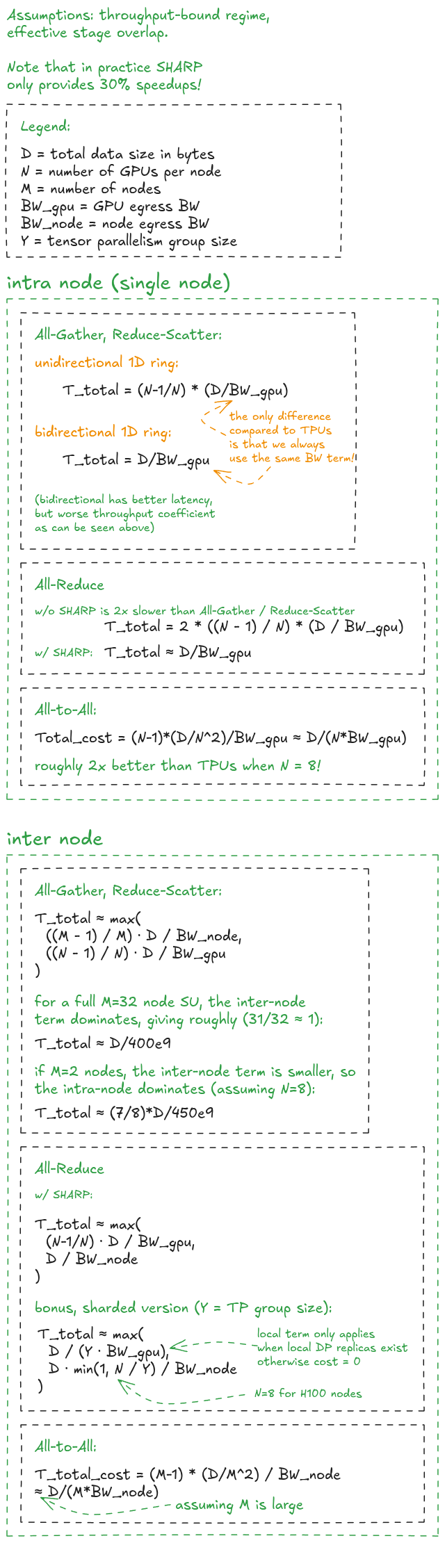
Figure 35: Summary of GPU collective communication costs for intra-node and inter-node collectives
Epilogue
尾声
Phew, that was a long one!
呼,这篇可真够长的!
What originally started as “let me maybe just make four figures covering All-Gather, Reduce-Scatter, All-Reduce, and All-to-All so I can understand them better, it shouldn’t take more than a day, right, right” somehow turned into this.
一开始它只是“我干脆画四张图,把 All-Gather、Reduce-Scatter、All-Reduce 和 All-to-All 讲清楚,好让自己理解得更透,不会超过一天吧,对吧,对吧”,不知怎么就变成了现在这样。
Along the way, I realized that the collective algorithms only really make sense once you understand the underlying hardware topology. TPUs were a bit easier to reason about, but I couldn’t skip GPUs, I love them too much. Rings are cool, but I also wanted to understand tree algorithms. But also SHARP, and fat trees, and hierarchical collectives. :’)
写的过程中我意识到,只有先理解了底层硬件拓扑,集合通信算法才真正讲得通。TPU 稍微好推理一些,但我又没法跳过 GPU——我太喜欢它们了。ring 很酷,可我还想搞懂 tree 算法。还有 SHARP、fat tree,以及分层集合通信。:’)
So the scope slowly expanded, and little by little, this blog post came to fruition. Just a side-quest.
于是范围慢慢扩大,一点一点地,这篇博客就成了现在的样子。就当是个支线任务吧。
Hope you liked it! :)
希望你喜欢!:)
💡 Get in touch:
If you spot any errors in the post, please DM me - feel free to drop me a message on X or LinkedIn or via anon feedback.
Acknowledgements
致谢
Thanks to my friends Aroun Demeure (ex GPU & AI at Magic, and ex-GPU architect at Apple and Imagination), Axel Feldmann (ML perf engineer at Jane Street), and Pranjal Shankhdhar (prev. GPU kernel engineer at xAI) for reading pre-release version of this blog post and providing feedback!
感谢我的朋友们 Aroun Demeure(前 Magic 的 GPU & AI、前 Apple 和 Imagination 的 GPU 架构师)、Axel Feldmann(Jane Street 的 ML 性能工程师)和 Pranjal Shankhdhar(前 xAI 的 GPU kernel 工程师)阅读本文的发布前版本并提供反馈!
Arun broadened the GPU discussion beyond balanced All-to-All, highlighting NVL72’s any-to-any topology, sparse and imbalanced MoE routing, and NVLink SHARP’s memory-style multicast/reduction model and practical trade-offs.
Arun 把 GPU 的讨论拓展到了均衡 All-to-All 之外,指出了 NVL72 的 any-to-any 拓扑、稀疏且不均衡的 MoE 路由,以及 NVLink SHARP 那种 memory-style 的组播/规约模型和它的实际取舍。
Axel refined the GPU section by highlighting rail optimization and SHARP’s SM/HBM offload benefits, then grounding the performance discussion with H100 measurements showing roughly 1.3× practical SHARP speedups and near-saturated collective bandwidth at around 1 GB.
Axel 通过点出 rail 优化和 SHARP 把规约卸载到 SM/HBM 之外的好处,进一步完善了 GPU 部分,并用 H100 上的实测把性能讨论落到实处:SHARP 的实际加速约为 1.3×,集合通信带宽在 1 GB 左右就接近饱和。
Pranjal independently reinforced the points on rail optimization and the gap between SHARP’s theoretical 2× speedup and the roughly 30% improvement typically observed in practice.
Pranjal 独立地印证了 rail 优化的要点,以及 SHARP 理论上的 2× 加速与实践中通常观察到的约 30% 提升之间的差距。
- “TPU 8t and TPU 8i technical deep dive”, https://cloud.google.com/blog/products/compute/tpu-8t-and-tpu-8i-technical-deep-dive
- “TPU topology visualizer”, https://tpu-visualizer.uc.r.appspot.com/
- “How to Scale Your Model”, https://jax-ml.github.io/scaling-book/
- “NVSwitch Hot Chips 2022”, https://hc34.hotchips.org/assets/program/conference/day2/Network%20and%20Switches/NVSwitch%20HotChips%202022%20r5.pdf
- “How to Scale Your Model: GPUs / intra-node collectives”, https://jax-ml.github.io/scaling-book/gpus/#intra-node-collectives
- Axel independently re-ran the benchmark using NCCL 2.29.7 on a 32-GPU H100 InfiniBand setup, corroborating the reported result: he likewise observed only a ~1.3× speedup on a 4 GB All-Reduce. Pranjal also reported the same result. Arun said this is more of a NCCL problem than a SHARP problem.
讨论
这里是静态站点,没有内嵌评论区。如果这篇文章对你有用,欢迎通过 RSS 订阅后续更新。